
ECA Lab manual
Dept of ECE, Lendi Institute of Engineering and Technology Page 1
LENDI INSTITUTE OF ENGINEERING AND
TECHNOLOGY
(Approved by AICTE, New Delhi and Affiliated to JNTU, Kakinada)
Department of Electronics & Communication Engineering
ELECTRONIC CIRCUIT ANALYSIS LAB
Lab Manual
Prepared by

ECA Lab manual
Dept of ECE, Lendi Institute of Engineering and Technology Page 2
LIST OF EXPERIMENTS
A) TESTING IN THE HARDWARE LABORATORY:
.
1. TWO STAGE RC COUPLED AMPLIFIER.
2. RC PHASE SHIFT OSCILLATOR USING TRANSISTORS.
3. CLASS A POWER AMPLIFIER.(SERIES FED)
4. CLASS B COMPLEMENTARY SYMMETRY AMPLIFIER.
5. CURRENT SHUNT FEEDBACK AMPLIFIER.
6. SINGLE TUNED VOLTAGE AMPLIFIER.
7.HARTELY OSCILLATOR
8.VOLTAGE SERIES FEED BACK AMPLIIER
9.CLASS –A TRANSORMER COUPLED POWER AMPIFIER
10.CLASS-B PUSHPULL POWER AMPLIFER
B) DESIGN AND SIMULATION USING PSPICE SOTWARE:
1. TWO STAGE RC COUPLED AMPLIFIER.
2. RC PHASE SHIFT OSCILLATOR USING TRANSISTORS.
3. CLASS B COMPLEMENTARY SYMMETRY AMPLIFIER
4.WEIN BRIDGE OSCILLATOR
5. CLASS A POWER AMPLIFIER.(SERIES FED)
6. SINGLE TUNED VOLTAGE AMPLIFIER.
7. CLASS –A TRANSORMER COUPLED POWER AMPIFIER
8.VOLTAGE SERIES FEED BACK AMPLIIER
9. CURRENT SHUNT FEEDBACK AMPLIFIER.
10.CLASS-B PUSHPULL POWER AMPLIFER

ECA Lab manual
Dept of ECE, Lendi Institute of Engineering and Technology Page 3
1. TWO STAGE RC COUPLED AMPLIFIER
AIM: To obtain the
V
oltage gain
f
o
r
two stage RC coupled
A
mpli
f
ie
r
and al
s
o to ob
s
e
r
ve
the
fr
equencyRe
s
pon
s
e.
.
EQUIPMENT REQUIRED:
1. cathode ray oscilloscope 1No
2.Regulated power supply 1No
3. function generator 1No
4.bread board 1No
5.connecting wires
COMPONENTS REQUIRED:
1. Resistors:
15k-2no
10k-2no
1k-2no
3.3k-2no
220Ω-2no
2.Transistor :BC107-2no
3.Capacitors-10µf -5no
CIRCUIT DIAGRAM:

ECA Lab manual
Dept of ECE, Lendi Institute of Engineering and Technology Page 4
THEORY: Wheneve
r
la
r
ge ampli
f
ication
w
ith ve
r
y good impedance matching i
s
r
equi
r
ed u
s
ing an active device
s
uch a
s
a t
r
an
s
i
s
to
r
o
r
a
f
ield e
ff
ect t
r
an
s
i
s
to
r
a
s
ingle
active device and it
s
a
ss
ociated ci
r
cuit
r
y
w
ill not be able to cate
r
to the need
s
.
I
n
s
uch
a ca
s
e
s
ingle
s
tage ampli
f
ie
r
i
s
not
s
u
ff
icie
n
t and one
r
equi
r
e
s
mo
r
e
s
tage
s
o
f
ampli
f
ication i.e., output o
f
one
s
tage i
s
connected to the input o
f
s
econd
s
tage o
f
ampli
f
ication ci
r
cuit and the chain continue
s
until the
r
equi
r
ed cha
r
acte
r
i
s
tic
s
o
f
ampli
f
ie
r
i
s
achieved
s
uch an ampli
f
ie
r
i
s
called a
s
multi
s
tage ampli
f
ie
r.I
n multi
s
tage
ampli
f
ie
r
, the output
s
ignal p
r
eceding
s
tage i
s
to be coupled to the input ci
r
cuit o
f
s
ucceeding
s
tage.
F
o
r
thi
s
inte
rs
tage coupling di
ff
e
r
ent type
s
o
f
coupling can be
employed. They a
r
e
1. RC coupling
2. T
r
an
sf
o
r
me
r
coupling
3.
D
i
r
ect coupling
RC coupling i
s
mo
s
t popula
r
ly u
s
ed type o
f
coupling becau
s
e it i
s
cheap and
p
ro
vide
s
excellent
f
idelity ove
r
a
w
ide
r
ange o
f
fr
equency .it i
s
u
s
ually employed
f
o
r
voltage.
PROCEDURE:
1
)
Connect the ci
r
cuit a
s
s
ho
w
n in the
f
igu
r
e.
2
)
A
p
p
ly 1
Khz frequencyand 20mv Vp-p
S
ine
w
ave
fr
om
f
unction
gene
r
ato
r
..
3
)
O
b
s
e
r
ve input and output Wave
f
o
r
m
s
s
imultaneou
s
ly on C.R.
O
4
)
Change the
fr
equency o
f
input
s
ignal
fr
om 10
H
Z to 1
MH
Z in
s
tep
s
and note amplit
u
de
s
o
f
input and output Wave
f
o
r
m
s(
input
s
ignal
s
hould be maintained con
s
tant
).
5
)
Calculate
V
oltage gain
(A)
f
o
r
each
(
in db
)
ve
rs
e
s
fr
equency.
Observations:
S.No
Frequenc
y ( Hz)
Input
Voltage
Output
Voltage
Gain=(V
0
/V
i
)
Gain in db=
20 log
10
(V
0
/V
i)

ECA Lab manual
Dept of ECE, Lendi Institute of Engineering and Technology Page 5
PRECAUTIONS:
1. Check connection
s
be
f
o
r
e
sw
itching
ON
po
w
e
r
s
upply.
2.
D
o
n’
t apply ove
r
voltage
3. When you a
r
e not u
s
ing the eq
u
ipment
sw
itch them
Off
CALCULATIONS
:
Maximum gain of the amp:
Upper cutoff frequency F2:
Lower cutoff frequency F1:
Band width=F2-F1:

ECA Lab manual
Dept of ECE, Lendi Institute of Engineering and Technology Page 6
EXPECTED GRAPH:
Input wave form
Output waveform
Frequeny response:

ECA Lab manual
Dept of ECE, Lendi Institute of Engineering and Technology Page 7
RESULT: -
1. Frequency response of Two stage RC coupled amplifier is plotted.
2. Gain = _______dB (maximum).
3. Bandwidth= fH--fL = _________Hz. At stage 2
VIVA QUESTIONS:
1.What is an amplifier?
2.what are the coupling elements of n this amplifier?
3.what are the applications of this amplifier?
4.why this type of amplifier will be used in AF mplifiers?
5.which type of biasing isused in this amplifier?
6.whatis the range of bandwidth in this amplifier?
Redraw the circuit diagram

ECA Lab manual
Dept of ECE, Lendi Institute of Engineering and Technology Page 8
2. RC PHASE SHIFT OSCILATOR USING TRANSISTORS
AIM: To calculate the frequency of the RC phase shift oscillator & to measure the phase
angles at different RC sections.
APPARATUS:
1. Transistor BC107
2. Resistors: 10KΩ -3Nos
8KΩ or 10KΩ
22KΩ
1.2KΩ
100KΩ
3. Capacitors: 0.001µf – 3 Nos
10µF – 2Nos
1µf
4. Regulated power Supply
5. CRO
THEORY:
RC-Phase shift Oscillator has a CE amplifier followed by three sections of RC phase
shift feedback Networks the output of the last stage is return to the input of the amplifier. The
values of R and C are chosen such that the phase shift of each RC section is 60º.Thus The RC
ladder network produces a total phase shift of 180º between its input and output voltage for
the given frequencies. Since CE Amplifier produces 180 º phases shift the total phase shift
from the base of the transistor around the circuit and back to the base will be exactly 360º or
0º. This satisfies the Barkhausen condition for sustaining oscillations and total loop gain of
this circuit is greater than or equal to 1, this condition used to generate the sinusoidal
oscillations.
The frequency of oscillations of RC-Phase Shift Oscillator is,
1
f = -----------
2RC* √6

ECA Lab manual
Dept of ECE, Lendi Institute of Engineering and Technology Page 9
CIRCUIT DIAGRAM:
PROCEDURE:
1. Make the connection as per the circuit diagram as shown above.
2. Observe the output signal and note down the output amplitude and time period (T
d
).
3. Calculate the frequency of oscillations theoretically and verify it practically (f=1/T
d
).
4. Calculate the phase shift at each RC section by measuring the time shifts (T
p
) between
the final waveform and the waveform at that section by using the below formula.
OBSERVATIONS:
THEORITICAL CALCULATIONS: R = 10KΩ, C = 0.001 μf
1
f = -------------- =
2RC* √6
PRACTICAL CALCULATIONS:
T
d
=
1
f = -----
T
d
Tp
1
(1). θ
1
= --------*360
0
=
T
d

ECA Lab manual
Dept of ECE, Lendi Institute of Engineering and Technology Page 10
Tp
2
(2). θ
2
= ------- * 360
0 =
T
d
Tp
3
(3). θ
3
= ----------- *360
0
=
T
d
MODEL WAVE FORMS:
OUT PUT WAVE FORM :
OUT PUT WAVE FORM : θ = 60
0
OUT PUT WAVE FORM : θ = 120
0
OUT PUT WAVE FORM : θ = 180

ECA Lab manual
Dept of ECE, Lendi Institute of Engineering and Technology Page 11
RESULT: The frequency of RC phase shift oscillator is calculated and the phase shift at
different RC sections is noted.
F
T
= F
P =
VIVA QUESTIONS:
1. What are the conditions of oscillations?
2. Give the formula for frequency of oscillations?
3. What is the total phase shift produce by the RC ladder network?
4. Whether the oscillator is positive feedback or negative feedback?
5. What are the types of oscillators?
6. What is the gain of RC phase shift oscillator?
7. What is the difference between damped oscillations undamped oscillations?
8. What are the applications of RC oscillations?
9. How many resistors and capacitors are used in RC phase shift network
10. How the Barkhausen criterion is satisfied in RC phase shift oscillator
REDRAW THE CIRCUIT DIAGRAM:

ECA Lab manual
Dept of ECE, Lendi Institute of Engineering and Technology Page 12
3.CLASS A POWER AMPLIFIER(SERIES FED)
AIM: To de
s
ign and te
s
t the cla
ss
A
po
w
e
r
ampli
f
ie
r
APPARATUS:
1. Class A power amplifier trainer kit
2. Function Generator
3. CRO
4. BNC Probes and connecting wires
CIRCUIT DIAGRAM:
THEORY:
The ampli
f
ie
r
i
s
s
aid to be cla
ss
A
po
w
e
r
ampli
f
ie
r
i
f
the q point and the input
s
ignal a
r
e
s
elected
s
uch that the output
s
ignal i
s
obtained
f
o
r
a
f
ull input cycle.
F
o
r
thi
s
cla
ss
the po
s
ition o
f
q point i
s
app
r
oximately y at the midpoint o
f
the load line.
F
o
r
all the value
s
o
f
input
s
ignal the t
r
an
s
i
s
to
r
r
emain
s
in the active
r
egion and neve
r
enti
r
e into the cut
off
o
r
s
atu
r
ation
r
egion. The collecto
r
cu
rr
ent
f
lo
ws
f
o
r
3600
(
li
f
e
cycle
)
o
f
the input
s
ignal in othe
r
w
o
r
d
s
the angle o
f
the collecto
r
cu
rr
ent
f
lo
w
i
s
3600 the class a ampli
f
ie
rs
o
r
f
u
r
the
rs
cla
ss
i
f
ied a
s
di
r
ectly coupled and t
r
an
sf
o
r
me
r
coupled and t
r
an
sf
o
r
me
r
coupled ampli
f
ie
rs
in di
r
ectly coupled type .The load i
s
di
r
ectly connected i
n
the collecto
r
ci
r
cuit
w
hile in the t
r
an
sf
o
r
me
r
coupled type, the
load i
s
coupled to the collecto
r
u
s
ing the t
r
an
sf
o
r
me
r
.
A
dvantage
s
:
1.
D
i
s
to
r
tion analy
s
i
s
i
s
ve
r
y impo
r
tant
2.
I
t ampli
f
ie
s
audio
fr
equency
s
ignal
s
f
aith
f
ully hence they a
r
e called a
s
audio
ampli
f
ie
rs

ECA Lab manual
Dept of ECE, Lendi Institute of Engineering and Technology Page 13
D
i
s
advantage
s
:
1.
H
pa
r
amete
r
analy
s
i
s
i
s
not applicable
2.
D
ue to la
r
ge po
w
e
r
handling the t
r
an
s
i
s
to
r
i
s
u
s
ed po
w
e
r
t
r
an
s
i
s
to
r
w
hich i
s
la
r
ge i
n
s
ize and having la
r
ge po
w
e
r
r
ating.
PROCEDURE:
1.
Switch
ON
Cla
ss
–
A
po
w
e
r
ampli
f
ie
r
t
r
aine
r
2.
S
et
Vs
(s
ay 250 to 300 m
V)
, at 10
KH
z u
s
ing
s
ignal gene
r
ato
r
.
3. Connect milli ammete
r
to the ammete
r
te
r
minal
s
4. By keeping the input voltage con
s
tant, va
r
y the
fr
equency
fr
om 0 to 1
MH
z
in
r
egula
r
s
tep
s
.
5.
N
ote do
w
n the co
rr
e
s
ponding output voltage
fr
om CR
O
6. Calculate the
D
C input po
w
e
r
u
s
ing the
f
o
r
mula
P
dc=
V
cc
I
c
7. Calculate the
A
C output po
w
e
r
u
s
ing the
f
o
r
mula
P
ac =
V
O
2
/8R
L
8. Calculate the e
ff
iciency η =
P
ac /
P
dc
9.
P
lot the g
r
aph bet
w
een
G
ain
(
db
)
and
fr
equency.
10. Calculate band
w
idth
fr
om the g
r
aph.
PRECAUTIONS:
1. Check connection
s
be
f
o
r
e
sw
itching
ON
po
w
e
r
s
upply
2.
D
on
’
t apply ove
r
voltage
3. When you a
r
e not u
s
ing the equipment
sw
itch them
OFF
.
4.
H
andle all equipment ca
r
e
f
ully.
CALCULATIONS:
Input power:
P
dc=
V
cc
I
c =
Outpower:
P
ac =
V
PP
2
/8R
L =
η = Efficiency=output power/input power*100 =
P
ac /
P
dc*100 =

ECA Lab manual
Dept of ECE, Lendi Institute of Engineering and Technology Page 14
EXPECTED GRAPH:
I/P:
O/P:
RESULT: Gain and
fr
equency a
s
ob
s
e
r
ved o
f
Cla
ss
A
po
w
e
r
ampli
f
ie
r
.
η = Efficiency=output power/input power*100 =
P
ac /
P
dc*100 =
VIVA QUESTIONS:
1.On which criteria based the power amplifiers are classified?
2.what is the operating point of class-A power ampliier?
3.what is meant by efficiency?
4.howmuch efficiency will b obtained in classs-A power amplifier?
5. what are the applications of power amplifier?
REDRAW THE CIRCUIT DIAGRAM:

ECA Lab manual
Dept of ECE, Lendi Institute of Engineering and Technology Page 15
4. CURRENT SHUNT FEEDBACK AMPLIFIER
AIM: To observe the performance of a current shunt feedback amplifier and obtain its
bandwidth.
EQUIPMENT RQUIRED:
Power supply 0-30V- 1 No.
CRO 20MHz - 1 No.
Digital multimeter - 1 No.
Signal generator 1Hz - 1MHz - 1 No.
COMPONENTS:
Resistors : 47K - 2 Nos.
2.2K - 2 Nos.
1K - 2 No
10K - 1No.
Capacitors 22µF - 3Nos.
0.1µF - 1No.
Transistors BC 107-2No.
THEORY:
Current shunt feedback circuit shows two transistor in cascade with feedback from the
second emitter to the first base through the resistor R
F
. we verify that this connection
produces negative feedback. The voltage V
i2
is much larger than V
i1
because of the voltage
gain of Q
1
. Also V
i2
is 180
0
out of phase with V
i1
. Because of emitter follower action V
e2
is
only slightly smaller than V
i2
, and these voltages are in phase. Hence V
e2
is larger in
magnitude than V
i1
and is 180
0
out of phase with V
i1
. If the input signal increases so that I
S
increases, If also increases, and I
i
= I
S
- I
f
is smaller than it would be their were no
feedback. This action is characteristics of negative feedback.
CIRCUIT DIAGRAM:

ECA Lab manual
Dept of ECE, Lendi Institute of Engineering and Technology Page 16
PROCEDURE:
1. Connect the circuit as shown in the figure
2. The operating points V
CEQ
, I
EQ
and V
BE
are measured.
3. Connect the signal generator with a sine wave of 1KHz frequency to the input and
increase the input to such a level that the output waveform of the signal as observed
on CRO is not distorted.
4. Measure the input and output voltages and calculate the gain of the amplifier. Av =
(V
O/P
/ V
I/P
).
5. To measure the input impedance, find the voltage drop across the known resistance
R
S.
The input current therefore is measured as the voltage across Rs / Rs value. Input
impedance Zi = Vi / Ii
6. To measure the input impedance, measure the output signal voltage V
O/P
without any
load. Connect a resistive load and then adjust the load until the new output signal V
O/P
equal to the one half of the original signal. Remove the R
OUT
from the circuit and
measure its value. The measured value is the output impedance of the circuit.
7. To measure the current gain A
I,
note down the output signal voltage when Ro is
connected and divide it by Ro to get the output current. Now current gain = output
current / input current. The power gain is the product of voltage gain and current gain.
8. Vary the frequency of the input signal from 50Hz to 1MHz in suitable steps and
calculate gain at each step. Plot the graph between voltage gain Vs frequency. Note
down the half power points and find the bandwidth of the amplifier.
9. Repeat the above steps by connecting (disconnecting) the emitter bypass capacitor C
E
.
The readings with C
E
give the response of the amplifier without out feedback. The
readings without the C
E
give the performance of the amplifier in current series
feedback mode.
MODEL GRAPHS:
A
V
max.
Gain in dB
Frequency
-3 dB point.
f
L
f
H
Bandwidth = f
H
-
f
L

ECA Lab manual
Dept of ECE, Lendi Institute of Engineering and Technology Page 17
Tabulation:
Without feedback:
S.No
Frequency
( Hz)
Input Voltage
Output Voltage
(V)
Gain(V
0
/V
i
)
20 log
10
(V
0
/V
i
)

ECA Lab manual
Dept of ECE, Lendi Institute of Engineering and Technology Page 18
With feedback:
S.No
Frequency
( Hz)
Input Voltage
Output Voltage
(V)
Gain(V
0
/V
i
)
20 log
10
(V
0
/V
i
)

ECA Lab manual
Dept of ECE, Lendi Institute of Engineering and Technology Page 19
RESULTS:
Without feedback
Input voltage (V
i
) =
Input frequency =
Output voltage (V
0
) =
Voltage gain =
Gain in dB = (20log
10
(V
0
/V
i
) =
With feedback
Input voltage (V
i
) =
Output voltage (V
0
) =
Voltage Gain =
Gain in dB = (20log
10
(V
0
/V
i
) =
CONCLUSIONS:
Conclusions can be drawn on comparing the voltage gain of the amplifier with and
without feedback, bandwidth obtained from the frequency response plot.
VIVA QUESTIONS:
1. What is the relationship between the transfer gain with feedback A
f
and that without feedback
A.
2. Define negative feedback.
3. Define the amount of feedback in decibels.
4. State the three fundamental assumptions which are made in order that the expression A
f
=
A/(1+A
) be satisfy exactly.
REDRAW THE CIRCUIT DIAGRAM:

ECA Lab manual
Dept of ECE, Lendi Institute of Engineering and Technology Page 20
5.SINGLE TUNED VOLTAGE AMPLIFIER
AIM: To study single tuned voltage Amplifier and to calculate
1. Resonant Frequency.
2. Q factor.
3. Bandwidth and
4. Impedance
APPARATUS:
1. Tuned RF Amplifier trainer Kit.
2. Function Generator.
3. CRO.
4. BNC probes and connecting wires
CIRCUIT DIAGRAM:
THEORY:
It is usually required to use a number of tuned amplifier stages in cascade in order to
obtain large overall gain. These cascade tuned amplifiers may be put into the following
three categories:
1. Single tuned amplifiers.
2. Double tuned amplifiers.
3. Stagger-tuned amplifiers.
Single tuned amplifiers use one parallel tuned circuit as the load impedance in each stage and
all these tuned circuits in different stages are tuned to the same frequency.Double tuned
amplifier uses two inductively coupled tuned circuits per stage, both the tuned circuits being
tuned to the same frequency.Staggered tuned amplifier uses a number of single tuned stages
in cascade, the successive tuned circuits being tuned to slightly different frequencies.
Single tuned amplifiers may again be put into following two categories:
a) Capacitance coupled single tuned amplifiers and

ECA Lab manual
Dept of ECE, Lendi Institute of Engineering and Technology Page 21
b) Transformer coupled or inductively coupled single tuned amplifiers
RESONANT FREQUENCY:
Depending upon the frequency of the source voltage Vs, the circuits may behave either as
inductive or capacitive. However, at a particular frequency when the inductive reactance Xl
equals the capacitive reactance Xc, then the circuit behaves as a purely resistive circuit. This
phenomenon is called resonance: and the corresponding frequency is called resonant
frequency. The resonant frequency (fr) can be found by equating the two reactance values.
PROCEDURE:
1. Connect ions should be made as per the circuit diagram.
2. Connect the AC signal source from function generator (above AF range) to input of the
trainer kit.
3. Keep the input voltage constant , vary the frequency in regular steps and down the
corresponding output voltage
4. Calculate the resonant frequency.
5. Plot the graph: gain (db) Vs frequency
6. Find the input and output impedance
7. Calculate the bandwidth and Q factor
PRECAUTIONS:
1. Check connections before switching ON power supply
2. Don’t apply over voltage
3. When you are not using the equipment switch them OFF.
4. Handle all equipment carefully
EXPECTED GRAPH:
Observations:
Input Voltage= (Constant)
S.NO
Input Frequency
(Hz)
OutputVoltage(V
o
)
Gain A = V
o-
/V
i
Gain in dB
20log(V
o
/V
i
)

ECA Lab manual
Dept of ECE, Lendi Institute of Engineering and Technology Page 22
RESULT: Gain and frequency as observed of single tuned voltage amplifier.
F
T
= F
P
=
VIVA QUESTIONS:
1. What are tuned amplifiers?
2. What is tuning?
3. Explain how the tuned amplifiers work?
REDRAW THE CIRCUIT DIAGRAM:

ECA Lab manual
Dept of ECE, Lendi Institute of Engineering and Technology Page 23
7.CLASS B COMPLEMENTARY SYMMETRY AMPLIFIER
AIM: To observe the input and output waveforms and to calculate the efficiency of Class B
Complimentary symmetry power amplifier.
APPARATUS:
EQUIPMENT REQUIRED:
Power supply 0-30V- 1 No.
CRO 20MHz - 1 No.
Digital multimeter - 1 No.
Signal generator 1Hz - 1MHz - 1 No.
COMPONENTS:
Resistors : 2.2K - 2 Nos.
100 - 2 Nos.
1K - 1 No
Transistors CL100- 1No , CK100 -1NO
CIRCUIT DIAGRAM:
THEORY:
An amplifying system consists of several stages in cascade. The input and the
intermediate stages amplify small signal excitations to a value large enough to drive the final
device .The out put stage feeds the final device .The output stage feeds a transducer such as a
CRO,loudspeaker or servomotor. Thus the final stage must be capable of delivering a large
voltage or current or appreciable amount of power. This requires an amplifier which is referred as
a power amplifier

ECA Lab manual
Dept of ECE, Lendi Institute of Engineering and Technology Page 24
In class B complimentary symmetry class _B amplifier one n-p-n and p-n-p is used. Hence the
circuit is called class-B complimentary symmetry amplifier. This circuit ifis transformer less
circuit .But with common emitter configuration it becomes power transfer without output
impedance for maximum power transfer without an output transformers. Hence the matched pair
of complementary transistors are used in common collector configuration This is because in
common collector configuration has lowest output impedance and hence the impedance matching
is possible.
PROCEDURE:
1.conncet the circuit s per the circuit diagram
2.apply 4v p-p with 1KHZ frequency using function generator
3.observe the output in CRO .
4.note the cross over distortion in output.(outputVp-p)
5.remove the collector connection and put ammeter.
6.note the Idc value in the ammeter.
7.using Pdc and Pac formulas find the efficiency.
OBSERVATION:
Pac=Vm2/2RL =
Pdc=Vcc*Idc =
VO =
VCC =
RL =
EFFICIENCY: η =Pac/Pdc*100=
MODEL GRAPHS: I/P WAVEFORM
ECA Lab manual
Dept of ECE, Lendi Institute of Engineering and Technology Page 25
O/P WAVEFORM
Vivavoice:
1.In classB power amplifiers why crossover distortion will be occurred?
2.what are he different methods to eliminate distortion?
3..howmuch efficiency will b obtained in classs-B power amplifier?
4.where is the location of operating point in class-B power amplifier?
REDRAW THE CIRCUIT DIAGRAM:

ECA Lab manual
Dept of ECE, Lendi Institute of Engineering and Technology Page 26
7. HARTLEY OSCILLATOR
AIM: To study and calculate frequency of oscillations of Hartley oscillator. Compare the
frequency of oscillations, theoretically and practically.
APPARATUS:
Hartley Trainer kit
Connecting wires
CIRCUIT DIAGRAM:
THEORY:
Hartley oscillator is very popular and is commonly used as a local oscillator in radio
receivers. It has two main advantages viz... Adaptability to wide range of frequencies and
easy to tune. The tank circuit is made up of L1, L2, and C1. The coil L1 is inductively
coupled to coil L2, the combination functions as auto transformer. The resistances R2 and R3
provide the necessary biasing. The capacitance C2 blocks the d.c component. The frequency
of oscillations is determined by the values of L1, L2 and C1 and is given by,

ECA Lab manual
Dept of ECE, Lendi Institute of Engineering and Technology Page 27
F=1/(2(C1(√L1+L2)))
The energy supplied to the tank circuit is of correct phase. The auto transformer provides
180˚ out of phase. Also another 180˚ is produced By the transistor. In this way, energy
feedback to the tank circuit is in phase with the generated oscillations.
PROCEDURE:
1. Connections are made as per the circuit diagram.
2. Connect CRO at output terminals and observe wave form.
3. Calculate practically the frequency of oscillations by using the Expression.
F=1/T, Where T= Time period of the waveform
4. Repeat the above steps 2, 3 for different values of L1 and note Down practical values of
oscillations of colpitts oscillator.
5. Compare the values of frequency of oscillations both theoretically And Practically.
OBSERVATIONS:
CAPACITANCE(μF),
INDUCTANCE(mH)
Theoritical frequency (KHZ)
Practical frequency (KHZ)
MODEL GRAPH:

ECA Lab manual
Dept of ECE, Lendi Institute of Engineering and Technology Page 28
RESULT: Frequency of oscillations is calculated and compared with theoretical values.
F(theoretical) = 1/2 ГLC=
F(practicl) =
VIVA QUESTIONS:
1. What are the applications of LC oscillations?
2. What type of feedback is used in oscillators?
3. What the expression for frequency of oscillations?
4. Whether an oscillator is dc to ac converter?
5. What is the loop gain of an oscillator?
6. What is the difference between amplifier and oscillator?
7. What is the condition for oscillations?
8. How many inductors and capacitors are used in Hartley Oscillator?
9. How the oscillations are produced in Hartley oscillator?
10. What is the difference between damped oscillations undamped oscillations?
REDRAW THE CIRCUIT DIAGRAM:

ECA Lab manual
Dept of ECE, Lendi Institute of Engineering and Technology Page 29
8. CLASS -A POWER AMPLIFIER(TRANSFORMER COUPLED)
AIM: To
o
b
s
e
r
ve the input and outp
u
t
w
ave
f
o
r
m
s
and to calculate the e
ff
iciency.
EQUIPMENT REQUIRED:
APPARATUS REQUIRED:
Power supply 0-30V- 1 No.
CRO 20MHz - 1 No.
Digital multimeter - 1 No.
Signal generator 1Hz - 1MHz - 1 No.
COMPONNTS REQUIRED:
Resistors 33KΩ - 1N0
5.6KΩ -2NO
470Ω -1NO
Capacitors 47uf -1NO
2.2uf - 1NO
TRANSFORMER -1NO
CIRCUIT DIAGRAM:
THEORY:
The ampli
f
ie
r
i
s
s
aid to be cla
ss
A
po
w
e
r
ampli
f
ie
r
i
f
the q point and the input
s
ignal a
r
e
s
elected
s
uch that the output
s
ignal i
s
obtained
f
o
r
a
f
ull input cycle .
F
o
r
thi
s
cla
ss
the po
s
ition o
f
q point i
s
app
r
oximately y at the mid point o
f
the load line.
F
o
r
all the value
s
o
f
input
s
ignal the t
r
an
s
i
s
to
r
r
emain
s
in the active
r
egion and
neve
r
enti
r
e into the cuto
ff
o
r
s
atu
r
ation
r
egion. The collecto
r
cu
rr
ent
f
lo
ws
f
o
r
3600
(
li
f
e cycle
)
o
f
the input
s
ignal in othe
r
w
o
r
d
s
the angle o
f
the collecto
r
cu
rr
ent
f
lo
w
i
s
3600 the claa a ampli
f
ie
rs
o
r
f
u
r
the
rs
cla
ss
i
f
ied a
s
di
r
ectly coupled and t
r
an
sf
o
r
me
r
coupled and t
r
an
sf
o
r
me
r
coupled ampli
f
ie
rs
in di
r
ectly coupled type .The load i
s
di
r
ectly connected in the collecto
r
ci
r
cuit
w
hile in the t
r
an
sf
o
r
me
r
coupled type,
the l
o
ad i
s
coupled to the collecto
r
u
s
ing the t
r
an
sf
o
r
me
r
.
A
dvantage
s
:

ECA Lab manual
Dept of ECE, Lendi Institute of Engineering and Technology Page 30
1.
D
i
s
to
r
tion analy
s
i
s
i
s
ve
r
y impo
r
tant
2.
I
t ampli
f
ie
s
audio
fr
equency
s
ignal
s
f
aith
f
ully hence they a
r
e called a
s
audio ampli
f
ie
rs
D
i
s
advantage
s
:
1.
H
pa
r
amete
r
analy
s
i
s
i
s
not applicable
2.
D
ue to la
r
ge po
w
e
r
handling the t
r
an
s
i
s
to
r
i
s
u
s
ed po
w
e
r
t
r
an
s
i
s
to
r
w
hich i
s
la
r
ge in
s
ize and having la
r
ge po
w
e
r
r
ating
PROCEDURE:
1.CONNCECT the circuit as per the ciecuit diadram
2.
S
et
Vs
(s
ay 250 to 300 m
V)
, at 10
KH
z u
s
ing
s
ignal gene
r
ato
r
.
3. Connect milli ammete
r
to the ammete
r
te
r
minal
s
4. By keeping the input voltage con
s
tant, va
r
y the
fr
equency
fr
om 0 to 1
MH
z
in
r
egula
r
s
tep
s
.
5.
N
ote do
w
n the co
rr
e
s
ponding output voltage
fr
om CR
O
6. Calculate the
D
C input po
w
e
r
u
s
ing the
f
o
r
mula
P
dc=
V
cc
I
c
7. Calculate the
A
C output po
w
e
r
u
s
ing the
f
o
r
mula
P
ac =
V
O
2
/8R
L
8. Calculate the e
ff
iciency n =
P
ac /
P
dc
9.
P
lot the g
r
aph bet
w
een
G
ain
(
db
)
and
fr
equency.
10. Calculate band
w
idth
fr
om the g
r
aph.
OBSERVATIONS:
VO
= ______________________________,
VI
= ____________________________
V
CC = ___
_
_________________________
RL = _____________________________
CALCULATIONS:
E
ff
iciency
(P
ac/
Pd
c
)
= __________________
P
ac
=
V
cc
I
c
P
DC
=
V
m
/2R
L
=
V
2
pp
/8R
L
%
n =
P
ac
/
P
DC
X
100

ECA Lab manual
Dept of ECE, Lendi Institute of Engineering and Technology Page 31
GRAPH: I/P
O/P
RESULT: Gain and
fr
equency a
s
ob
s
e
r
ved o
f
Cla
ss
A
po
w
e
r
ampli
f
ie
r
.
%
n =
P
ac
/
P
DC
X
100 =
VIVA QUESTIONS:
1.On which criteria based the power amplifiers are classified?
2.what is the operating point of class-A power ampliier?
3.what is meant by efficiency?
4.howmuch efficiency will b obtained in classs-A power amplifier?
5. what are the applications of power amplifier?
REDRAW THE CIRCUIT DIAGRAM:

ECA Lab manual
Dept of ECE, Lendi Institute of Engineering and Technology Page 32
9.VOLTAGE-SERIES FEEDBACK AMPLIFIER
AIM: To study the effect of voltage series feedback on Gain of the Amplifier.
APPARATUS:
Transistor BC 107 -1no
Breadboard
Regulated Power Supply(0-30V,1A)
Function Generator
CRO (30 Mhz,dualtrace)
Resistors 33kΩ,3.3k Ω,1.5kΩ,1kΩ-2no
Capacitors 10µF - 3Nos
CIRCUIT DIAGRAM:
THEORY:
When any increase in the output signal results into the input in such a way as to cause
the decrease in the output signal, the amplifier is said to have negative feedback. The
advantages of providing negative feedback are that the transfer gain of the amplifier with
feedback can be stablised against varations in the hybrid parameteresof the transistor or the
parameters of the other active devices used in the circuit. The most advantage of the negative
feedback is that by propere use of this , there is significant improvement in the frequency
respponse and in the linearity of the operation of the amplifier.This disadvantage of the
negative feedback is that the voltage gain is decreased.

ECA Lab manual
Dept of ECE, Lendi Institute of Engineering and Technology Page 33
In Voltage-Series feedback , the input impedance of the amplifier is decreased and the
output impedance is increased.Noise and distortionsare reduced cosiderably.
PROCEDURE:
1. Connections are made as per circuit diagram.
2. Keep the input voltage constant at 20mV peak-peak and 1kHz frequency.For different
values of load resistance, note down the output voltage and calculate the gain by using
the expression
A
v
= 20log(V
0
/ V
i
) dB
3. Add the emitter bypass capacitor and repeat STEP 2.And observe the effect of
Feedback on the gain of the amplifier
4. For plotting the frquency the input voltage is kept constant at 20mV peak-peak and
the frequency is varied from 100Hz to 1MHz.
5. Note down the value of output voltage for each frequency. All the readings are
tabulated and the voltage gain in dB is calculated by using expression A
v
= 20log(V
0
/
V
i
) dB
6. A graph is drawn by takung frquency on X-axis and gain on Y-axis on semi log graph
sheet
7. The Bandwidth of the amplifier is calculated from the graph using the expression
Bandwidth B.W = f
2
– f
1
.
Where f
1
is lower cutt off frequency of CE amplifier
f
2
is upper cutt off frequency of CE amplifier
The gain-bandwidth product of the amplifier is calculated by using the expression
Gain-Bandwidth Product = 3-dB midband gain X Bandwidth.
OBSERVATIONS:
Frequency Response with feedback: V
i
= 20mV
S.NO
Frequency (Hz)
OutputVoltage(V
o
)
Gain A =
V
o
/V
i
Gain in dB
20log(V
o
/V
i
)

ECA Lab manual
Dept of ECE, Lendi Institute of Engineering and Technology Page 34
MODEL WAVEFORMS:

ECA Lab manual
Dept of ECE, Lendi Institute of Engineering and Technology Page 35
Result:
Bandwidth(with feed back)=f2-f1
Viva voice:
1. what is meant by feed back?
2. what are the types of feed back?
3. why we are using negative feed back in feedback amplifiers?
4.what are the different types of feedback amplifiers?
REDRAW THE CIRCUIT DIAGRAM:

ECA Lab manual
Dept of ECE, Lendi Institute of Engineering and Technology Page 36
10.CLASS B PUSH PULL POWER AMPLIFIER
AIM: To observe the input and output waveforms and to calculate the efficiency of Class B
Complimentary symmetry power amplifier.
EQUIPMENT REQUIRED:
APPARATUS REQUIRED:
Power supply 0-30V- 1 No.
CRO 20MHz - 1 No.
Digital multimeter - 1 No.
Signal generator 1Hz - 1MHz - 1 No.
COMPONNTS REQUIRED:
Resistors 10KΩ - 1N0
1KΩ - 1NO
220Ω -1NO
Capacitors 0.47uf -1NO
22uf - 2NO
TRANSFORMER -2NO
CIRCUIT
DIAGRAM:
THEORY:
An amplifying system consists of several stages in cascade. The input and the intermediate stages
amplify small signal excitations to a value large enough to drive the final device .The out put
stage feeds the final device .The output stage feeds a transducer such as a CRO,loudspeaker or
servomotor. Thus the final stage must be capable of delivering a large voltage or current or
appreciable amount of power. This requires an amplifier which is referred as a power amplifier

ECA Lab manual
Dept of ECE, Lendi Institute of Engineering and Technology Page 37
In class B complimentary symmetry class _B amplifier one n-p-n and p-n-p is used. Hence the
circuit is called class-B complimentary symmetry amplifier. This circuit ifis transformer less
circuit .But with common emitter configuration it becomes power transfer without output
impedance for maximum power transfer without an output transformers. Hence the matched pair
of complementary transistors are used in common collector configuration This is because in
common collector configuration has lowest output impedance and hence the impedance matching
is possible.
PROCEDURE:
1.conncet the circuit s per the circuit diagram
2.apply 4v p-p with 1KHZ frequency using function generator
3.observe the output in CRO .
4.note the cross over distortion in output.(outputVp-p)
5.remove the collector connection and put ammeter.
6.note the Idc value in the ammeter.
7.using Pdc and Pac formulas find the efficiency.
OBSERVATION:
VO =
VCC =
RL =
EFFICIENCY: Pac/PDC = Vmx II /4 X VCC =
Vm = V pp/2
MODEL GRAPHS: I/P
O/P

ECA Lab manual
Dept of ECE, Lendi Institute of Engineering and Technology Page 38
RESULT: The efficiency of class B complimentary symmetry power amplifier is obtained.
EFFICIENCY: Pac/PDC = Vmx II /4 X VCC =
VIVA QUESTIONS:
1.In classB power amplifiers why crossover distortion will be occurred?
2.what are he different methods to eliminate distortion?
3..howmuch efficiency will b obtained in classs-B power amplifier?
4.where is the location of operating point in class-B power amplifier?
REDRAW THE CIRCUIT DIAGRAM:

ECA Lab manual
Dept of ECE, Lendi Institute of Engineering and Technology Page 39
INTRODUCTION TO PSPICE:
PSPICE is abbreviated as Personal Simulation Program with Integrated Circuit Emphasis.
PSpice is a SPICE analog circuit and digital logic simulation program.
SPICE (Simulated Program with Integrated Circuit Emphasis) is a general purpose software
that simulates different circuits and can perform various analysis of electrical and electronic
circuits including time domain response, small signal frequency response, total power
dissipation, determination of nodal voltages and branch current in a circuit, transient analysis,
determination of operating point of transistors, determinations of transfer functions etc. This
software is designed in such a way so that it can simulate different circuit operations
involving transistors, operational amplifiers (op – amp) etc. and contains models for circuit
elements (passive as well as active).
SPICE was first developed in the University of California, Berkeley, USA in early 1970s.
Subsequently an improved version SPICE 2 was available in the mid of 1970s especially to
support computer aided designs. In due course of time this program (SPICE 2 has become so
versatile in the industry that people used to call, this program itself as SPICE. PSpice is also
the member of SPICE family and it is a commercial software product based on SPICE
algorithm. It is useful for simulating all types of circuits in a variety of applications. In both
SPICE and PSpice, the circuit is described by statements those are stored in a file (namely
Circuit File). The SPICE simulator is assigned to read this file to run the simulation. In
PSpice, the statements are self – contained and independent; obviously they do not interact
with each other. The statements are also easy to learn and use. PSpice includes additional
features that make the program more flexible and user friendly. Notably among other features
is the graphics post processor probe which acts like a software oscilloscope and is capable of
exhibiting various waveforms. PSpice has become one of the most popular circuit simulation
programs. In order to draw the circuit and create a schematic file, schematic editor can be
used in the PSpice simulation.
PSpice is a part of larger software package called the Design Lab, originally developed by
MicroSim Corporation as the Design Centre. It is now marketed by Or CAD.
OVERVIEW:
Start a Project Draw a schematic Simulate circuit Graph data
Each part will be discussed in more detail in the next four sections.
1. STARTING A PROJECT
2. DRAWING A SCHEMATIC
1. Summary of PSpice Parts

ECA Lab manual
Dept of ECE, Lendi Institute of Engineering and Technology Page 40
2. What your Schematic Needs
3. Adding Parts to your Circuit
4. Using Wires
5. Adding a Ground
6. Changing the Value of a Part
7. Other Notes: Unique Names and Labeling Nodes
3. SIMULATING YOUR CIRCUIT
1. General Instructions
2. Bias Point (DC Calculations)
3. DC Sweep on Input Source, V
i
4. Parametric Sweep
5. AC Sweep (Frequency Domain Simulation)
6. Transient Analysis (Time Domain Simulation)
4. GRAPHING IN PSPICE
1. General Instructions
2. Bode Plot
5. MISCELLANEOUS ITEMS
1. Creating an IV Plot
2. Using the OpAmp
3. Family of Curves Option for Resistance
4. Using the Zener Diode
5. Creating a Potentiometer
1. STARTING A PROJECT
1) Open OrCAD Capture
2) Go to File => New => Project…
3) Enter a name
4) Choose "Analog or Mixed A/D"

ECA Lab manual
Dept of ECE, Lendi Institute of Engineering and Technology Page 41
5) Set the location. (You should create a new directory for your project since PSpice
will generate a bunch of project files in this folder.)
6) Click OK
7) Choose "Create blank project" and click OK
8) You should now see a window where you can draw the schematic (i.e., your circuit
diagram).
2. DRAWING A SCHEMATIC
2.1 Summary of PSpice Parts for ECE 65
PART
PART NAME
PICTURE
NOTES
DC Source
VDC / Source
AC Source
VAC / SOURCE

ECA Lab manual
Dept of ECE, Lendi Institute of Engineering and Technology Page 42
Sine Wave Source
VSIN / SOURCE
See Section 4.6 for
more instructions
Triangle Wave
Source
Square Wave Source
VPULSE / SOURCE
See Section 4.7 for
more instructions
Ground (ref. voltage)
0 / SOURCE
Resistor
R / ANALOG
Capacitor
C / ANALOG
Inductor
L / ANALOG
741 OpAmp
uA741 / EVAL
See Section 6.2 for
more instructions
Diode
D1N4148 / EVAL
Zener Diode
D1N5232 / EVAL
See Section 6.4 for
more instructions
npn BJT
Q2N3904 / BIPOLAR
2.2 What your Schematic Needs
All schematics you draw on PSpice will need the following: a voltage source, components,
wires, and a ground. The next couple of sections will instruct you on how to draw a full
circuit.
2.3 Adding Parts to your Circuit
1) Go to Place => Parts

ECA Lab manual
Dept of ECE, Lendi Institute of Engineering and Technology Page 43
2) Click on the library you want to use, or select multiple libraries by holding Ctrl or
dragging the mouse. In the parts window you should see at least the ANALOG, BIPOLAR,
EVAL, SOURCE, and SPECIAL libraries. If you don't see these libraries already listed, you
will need to add them:
a. Click Add Library…
b. Navigate to C:\Program Files\OrCad_Demo\Capture\Library\Pspice (This is the
location in the PSpice lab computers. The location may be different if you install PSpice
on your own computer, but find the ...\Capture\Library\Pspice folder)
c. Highlight all the *.olb files in this folder. You can hold Ctrl and click on the files, or
drag the mouse to select multiple files.
d. Click Open. You should now see a list of libraries in the "Libraries:" section.
3) Find the part you want to add and press OK.
4) Click where you want to place the part on your schematic. (Press R to rotate the part by
90 degrees)
5) When you are finished with the part, right click and select End Mode to return to the
pointer.
2.4 Using Wires
1) Select Parts => Wire. The pointer changes to a cross-hair.
2) Drag cursor from one connection point to another. Clicking on any valid
connection will end the wire.

ECA Lab manual
Dept of ECE, Lendi Institute of Engineering and Technology Page 44
3) Continue connecting the rest of the circuit.
4) When you are finished, right click the mouse and select End Wire to return to the
pointer. An example circuit from Lab 1 is shown below.
2.5 Adding a Ground
There are many types of grounds (common points in the circuit, noise reduction, etc.) PSpice
uses node-voltage method for circuit simulation and, therefore, needs a reference node with
“zero voltage”. This is the 0/source ground. You need to have it in your circuits! (It looks
like a ground symbol with a zero.) If you don't, PSpice may complain of "floating nodes"
even if you have a ground.
To place the ground on the circuit:
1) Go to Place => Ground. The ground you want to use is either listed as 0 or
0/source.

ECA Lab manual
Dept of ECE, Lendi Institute of Engineering and Technology Page 45
If you don't see the 0/source ground, you will need to add the "source" library:
a. Click Add Library…
b. Navigate to C:\Program Files\OrCad_Demo\Capture\Library\Pspice (This is the
location in the PSpice lab computers. The location may be different if you install PSpice
on your own computer, but find the ...\Capture\Library\Pspice folder)
c. Highlight source.olb.
d. Click Open. You should now see the “source” library and the 0/source ground.
2) Connect the ground to your circuit.
2.6 Changing the Value of a Part
For the parts above, V2 and R4 are the names of the components, while 0Vdc and 1k are the
values. To change a part’s value, double-click the value of the part. A new window will pop
up where you can type in the value you want.

ECA Lab manual
Dept of ECE, Lendi Institute of Engineering and Technology Page 46
2.7 Other Notes
1) All parts must have unique names. You can't have two parts named "R1" in your circuit.
If you are copying and pasting parts or circuits from another project, you will need to rename
your parts because PSpice doesn't do this automatically.
2) Labeling Nodes. I recommend you use aliases to label your input and output nodes. This
makes your node easier to find when you start plotting out your data. V(Vout) is simpler than
finding V(R1:1)
a. Go to Place => Net Alias
b. Enter a name, i.e., Vout or Vin
c. Place the label on the wire connected to the node.
An example of labeling from Lab 1 is shown below.
3. SIMULATING YOUR CIRCUIT
3.1 General Instructions
Special Characters
Meaning
Example
What to Type
M
milli (10
-3
)
10 mH
10m
K
kilo (10
3
)
1 kΩ
1k
MEG
mega (10
6
)
10 MΩ
10MEG

ECA Lab manual
Dept of ECE, Lendi Institute of Engineering and Technology Page 47
1) Go to PSpice => New Simulation Profile. Or if you already have a profile and would like
to edit it, go to Edit Simulation Profile
2) Choose the analysis type from the drop down menu.
3) Adjust the settings on the right hand side. More instructions are given in the next four
sections.
4) Press OK.
5) Go PSpice => Run. Or press the play button.
6) A new window (the simulation window) will pop up. Any errors from your circuit will be
displayed on the bottom left text window. Fix those errors before you continue. If there are
no errors, you are now ready to do one of two things: plot data on the simulation window or
display the DC calculations on your schematic.
3.2 Bias Point (DC Calculations)
1) Analysis Type: Bias Point
2) Options: General Settings
a. For Lab #7, you will also need to select Temperature (Sweep) to run the simulation at
different temperatures.
3) Output File Options: None
Press OK and then simulate your circuit. To display DC bias voltages and currents on your
circuit after you run the simulation, go to PSpice => Bias Points, and check Enable, Enable
Bias Current Display, and/or Enable Bias Voltage Display. You should now see values on
your circuit representing current and/or voltage.
3.3 DC Sweep on Input Source V
i
1) Analysis type: DC Sweep
2) Options: Primary Sweep
3) Sweep Variable: Voltage Source
4) Type in the name of the source you are sweeping.
5) Sweep Type: Linear (this is so you can sweep three a range of values)
6) Fill in the Start, End, and Increment Values. Type in 0.1V for the increment value to get a
nice smooth plot.
3.4 Parametric Sweep for Resistance
You will need to make the following changes to your circuit first:

ECA Lab manual
Dept of ECE, Lendi Institute of Engineering and Technology Page 48
1) Change the value of the part (not the name!) to {RL} (use curly braces, name is arbitrary)
2) Go to Place => Part
3) Add the part PARAM/SPECIAL to your schematic
4) Double click on the PARAM part
5) Click "New Column..."
6) Set the name to RL (same name as in “a” but with no curly braces)
7) Set the value to something, e.g., 1k (this is the value that is used in calculating DC bias
values, choose somewhere in the range of your sweep).
8) Select the RL column (do not double click!) so that it is highlighted and then click
Display...
9) Select "Name and Value" and press OK.
10) An example schematic from Lab 1 is shown below:
Simulation Settings:
1) Analysis type: DC Sweep
2) Options: Primary Sweep (not Parametric Sweep!)
3) Sweep variable: Global parameter
4) Parameter name: RL (or name of the parameter you used without curly braces)
5) Sweep Type: Linear
6) Fill in the Start, End, and Increment values. Note for resistance, the start value cannot be
0! Use 0.1 instead.
Press OK and simulate. The simulation window should now include a place for you to plot
your data.

ECA Lab manual
Dept of ECE, Lendi Institute of Engineering and Technology Page 49
3.5 AC Sweep (Frequency Domain Simulation)
1) Set up your circuit with VAC voltage sources.
2) Go to PSpice => New or Edit Simulation Profile
3) Analysis Type: AC Sweep/Noise
4) Sweep Type: choose logarithmic and decade. Then select the frequency range of interest.
Don't start frequency sweeps at 0!
5) Set the Points/Decade to be at least 20.
Press OK and simulate. The simulation window should now include a place for you to plot
your data.
3.6 Transient Analysis (Time Domain Simulation)
1) For a sine wave, use VSIN for your voltage source instead of VAC (VOFF is the DC
offset, VAMPL is the amplitude, and FREQ is the frequency of the sine wave).
2) For a square or triangular wave, use VPULSE . The values you type in for V1 and V2 will
depend on the amplitude specified on the lab instructions. If a 5V amplitude signal is
specified, then V1 = 5V and V2 = -5V.
a. Square Wave is the VPLUSE function in the limit of TR = TF = 0 and PW = 0.5 * PER
(PER is the period of the wave). This limit case, however, causes numerical difficulties in
calculations. In any case, we can never make such a square function in practice. In reality,
square waves have very small TR and TF. Typically, we use a symmetric function, i.e., we
set TR = TF and PW = 0.5 * PER - 2 * TR. Thus, for a given frequency we can set up the
square function if we choose TR. If we choose TR too large, the function does not look like a
square wave. If we choose TR too small, the program will take a long time to simulate the
circuit and for TR smaller than a certain value, the simulation will not converge numerically.
A good choice for TR is to set it to be 1% of the PER (a period): TR = TF = 0.01 * PER, PW
= 0.48 * PER. This usually results in a nice signal without a huge amount of computational
need. Note that TR does not have to be exactly 1% of PER. You can choose nice round
numbers for TR, TF, and PW.
b. Triangular Wave is the VPLUSE function in the limit of TR = TF = 0.5* PER and PW =
0 (convince yourself that this is the case). As before, the limit case of PW = 0 causes
numerical difficulties in calculations. So we have to choose PW to be a reasonably small

ECA Lab manual
Dept of ECE, Lendi Institute of Engineering and Technology Page 50
value. A good choice for PW is to be set at 1% of the PER (period): PW = 0.01* PER, TR =
TF = 0.49 * PER (and not TR = TF = 0.495 * PER so that we get a symmetric function). This
usually results in a nice signal without a huge amount of computational need. Again, note that
PW does not have to be exactly 1% of PER. You can choose nice round numbers for TR, TF,
and PW.
3) Simulation settings:
a. Analysis Type: Time Domain (Transient)
b. Options: General Settings
c. Enter a Run to time so that a few periods will be displayed. Remember that the period
(seconds) = 1/frequency (Hz), i.,e, if you are using a 1kHz sine wave, it has a 1/1kHz=1ms
period, so use a Run to time of 5ms for 5 periods
d. Set the Maximum step size to be much smaller than the period. i.,e, for a 1kHz sine
wave: It has a 1ms period, so set a maximum step size of approx .01ms. (This works out to
100 data points per period). If you don't set the maximum step size, PSpice may choose
one which is too big, making your sine wave look angular and ugly.
Press OK and simulate. The simulation window should now include a place for you to plot
your data.
4 GRAPHING IN PSPICE
4.1 General Instructions
On the simulation window,
1) Go to Trace => Add Trace
2) Select the variable you want to plot on the y-axis. Or type in an expression on the Trace
Expression prompt at the bottom of the window. Press OK
3) To mark points:
a. Click the "Toggle Cursor" button. (Or go through the menu, Trace => Cursor
=> Display.) You will now be able to move the cursor along your plot.
b. Click the "Mark Label" button to label that point. (Or go through the menu, Plot
=> Label => Mark.)
4.2 Bode Plots
1) For the magnitude plot, use the PSpice DB() function to convert the transfer function to
decibels. For example, you could type in DB(V(Vout)/V(Vin)) as your Trace Expression,

ECA Lab manual
Dept of ECE, Lendi Institute of Engineering and Technology Page 51
assuming you have labeled your output and input nodes with "Vout" and "Vin" aliases. Note
that DB(Vout) is NOT the transfer function in dB.
2) Next, mark the cutoff frequency on the magnitude plot. To find the cutoff frequency,
remember the cutoff frequency is 3dB below the highest point (NOT always at -3dB). Here
are some instructions on how to label the cutoff frequencies.
a. Click the "Toggle Cursor" button. (Or go through the menu, Trace => Cursor
=> Display.)
b. Click the "Cursor Max" button to find the highest point. (Or go through the menu,
Trace => Cursor => Max.)
c. Click the "Mark Label" button to label the max point. (Or go through the menu,
Plot => Label => Mark.) This point is the center frequency f
o
for a bandpass filter.
d. Click the "Cursor Search" button (Or go through the menu, Trace => Cursor
=>Search Commands…)
e. Select 1 for Cursor To Move to search along the y-axis
f. To find the cutoff frequency f
c
(or cutoff frequencies f
cl
and f
cu
for a bandpass filter),
enter "search forward level (max-3)" (don't enter the quotation marks) to move the cursor
to the right to the point which is 3dB below the max. Or enter "search back level (max-
3)" (don't enter the quotation marks) to move the cursor to the left
f. Click the "Mark Label" button to label that cutoff point.
Unclick the Toggle Cursor button to disable the cursor so you can move the label.
Double click on the label to edit the text (to add units, or to name the point)
3) Once you have completed the magnitude plot, you will now need to create a phase plot.
To put the plot on the same window for convenience, go to Plot => Add Plot to Window. To
graph the phase plot, use the PSpice P() function. For example, P(V(Vout)/V(Vin)).
4) To label the cutoff frequencies on the phase plot, simply search for the angles that
correspond to each cutoff frequency. You can find these in the class lecture notes. For

ECA Lab manual
Dept of ECE, Lendi Institute of Engineering and Technology Page 52
example, for a passive lowpass filter, the cutoff frequency is located where the phase shift is -
45 degrees. So on the plot, you would search for -45 and then label that point.
5) It may help to increase the width of the lines in the plot:
a. The colored symbol at the bottom of the graph, or on the graph line.
b. Note you can select all of the lines by going to Edit => Select All.
c. Right click on the line. Make sure the selection list has Information, Properties, Cursor
1, and Cursor 2. (If it lists Settings and Properties, you clicked on the background, not on
the line).
d. Select Properties.
e. You can change the width and other settings of that trace.
6) An example of a complete Bode plot with labels is shown below:
5. MISCELLANEUOUS ITEMS
5.1 Creating an IV Plot
Here, you will need to make a plot of current vs. voltage.
1) Use the same schematic and settings you made for a parametric sweep on the resistance.
2) Simulate the circuit.
3) On the simulation window, go to Trace => Add Trace.
4) Select the current through the load resistance. If you typed in RL as your parameter, the
variable you will choose will be I(RL).

ECA Lab manual
Dept of ECE, Lendi Institute of Engineering and Technology Page 53
5) Add a negative sign in the trace expression, so that you have –I(RL). You will need to do
this because you want the current going into the voltage divider circuit. Without the negative
sign, you will be plotting the current coming out of the voltage divider circuit.
6) Change the x-axis variable from resistance to voltage:
a. Go to Plot => Axis Setting
b. Under the X Axis tab, click Axis Variable…
c. Select the voltage across the load. This will probably be V2(RL) if RL is your
parameter name.
7) Press OK. Your graph should now be a plot of I vs. V.
5.2 Using the OpAmp
1) Connection points 2, 3, and 6 should be self-explanatory. See the circuit diagram in your
lab instructions to figure what to connect to these points.
2) Connection point 7: attach a VDC to supply power to the OpAmp and change the value to
15V. Don’t forget to ground the DC source by attaching the 0/source to the negative
terminal.
3) Connection point 4: attach a VDC to supply power to the OpAmp and change the value to
-15V. Don’t forget to ground the DC source by attaching the 0/source to the negative
terminal.
4) Do not connect anything to connection points 1 and 5.
5) An example circuit is shown on the next stage:

ECA Lab manual
Dept of ECE, Lendi Institute of Engineering and Technology Page 54
5.3 Family of Curves Option for Resistance
First, you will need to make changes to your circuit so that your resistance R2 is now a
parametric variable. Follow the first part of the instructions in section 4.4 on how to do this.
Do not follow the instructions for the simulation settings. You will need to follow these
instructions:
1) Analysis type: AC Sweep
2) Options: General Settings and Parametric Sweep
3) For General Settings,
a. AC Sweep Type: Logarithmic Decade
b. Fill in Start, End, and Points/Decade
4) For Parametric Sweep,
a. Sweep variable: Global parameter
b. Parameter name: R (or name of the parameter you used on the schematic minus the
curly braces)
c. Sweep type: Value list
d. Fill in the list box. Make sure to separate each value with a space and not a comma.
For example, you would type in 1k 2k 3k and not 1k, 2k, 3k.
Once you have set up the Sweep Type, press OK and then simulate your circuit. The
simulation window should now include a place for you to plot your data. See Section 5.
5.4 Using the Zener Diode
1) You need 2 files
a. D1N5232.lib (PSpice library file)
b. D1N5232.olb (Orcad Capture library file)
2) PSpice Instructions:
a. Go to the menu: 'PSpice => Edit Simulation Settings'
b. Go to the 'Libraries' tab. Click the 'Browse...' button. Open the D1N5323.lib file
c. Click 'Add as Global'
d. Press 'OK' to exit the simulation settings.
e. Now go to the menu: 'Place => Part...'

ECA Lab manual
Dept of ECE, Lendi Institute of Engineering and Technology Page 55
f. Click 'Add Library'
g. Open the D1N5232.olb file
h. You should now see a part named D1N5232. Select it and press OK to use the part.
5.5 Creating a Potentiometer
You will not need to use a special part for this. Simply perform a parametric sweep on a
regular resistor

ECA Lab manual
Dept of ECE, Lendi Institute of Engineering and Technology Page 56
1.TWO STAGE RC COUPLED AMPLIFIER
AIM: To plot the frequency response of a two stage RC –coupled amplifier using BJT and
calculate 3-db band width
APPARATUS:
PSPICE Simulation Software
THEORY:
Whenever large amplification with very good impedance matching is required using
an active device such as a transistor or a field effect transistor a single active device and its
associated circuitry will not be able to cater to the needs. In such a case single stage amplifier
is not sufficient and one requires more stages of amplification i.e., output of one stage is
connected to the input of second stage of amplification circuit and the chain continues until
the required characteristics of amplifier is achieved such an amplifier is called as multistage
amplifier In multistage amplifier, the output signal preceding stage is to be coupled to the
input circuit of succeeding stage. For this interstage coupling different types of coupling can
be employed. They are
1. RC coupling
2. Transformer coupling
3. Direct coupling
RC coupling is most popularly used type of coupling because it is cheap and provides
excellent fidelity over a wide range of frequency .it is usually employed for voltage
amplification .A coupling capacitor is connected to the output of first stage to the base of the
input of the second stage and so on.

ECA Lab manual
Dept of ECE, Lendi Institute of Engineering and Technology Page 57
CIRCUIT DIAGRAM:
DC SWEEP:

ECA Lab manual
Dept of ECE, Lendi Institute of Engineering and Technology Page 58
TRANSIENT:
AC SWEEP:

ECA Lab manual
Dept of ECE, Lendi Institute of Engineering and Technology Page 59
RESULT:
VIVA QUESTIONS:
1.What is an amplifier?
2.what are the coupling elements of n this amplifier?
3.what are the applications of this amplifier?
4.why this type of amplifier will be used in AF mplifiers?
5.which type of biasing isused in this amplifier?
6.whatis the range of bandwidth in this amplifier?

ECA Lab manual
Dept of ECE, Lendi Institute of Engineering and Technology Page 60
2.RC PHASE SHIFT OSCILLATOR
AIM: To calculate the frequency of the RC phase shift oscillator & to measure the phase
angles at different RC sections.
APPARATUS:
PSPICE Simulation Software
THEORY:RC-Phase shift Oscillator has a CE amplifier followed by three sections of RC
phase shift feed back Networks the out put of the last stage is return to the input of the
amplifier. The values of R and C are chosen such that the phase shift of each RC section is
60º.Thus The RC ladder network produces a total phase shift of 180º between its input and
output voltage for the given frequencies. Since CE Amplifier produces 180 º phases shift the
total phase shift from the base of the transistor around the circuit and back to the base will be
exactly 360º or 0º. This satisfies the Barkhausen condition for sustaining oscillations and total
loop gain of this circuit is greater than or equal to 1, this condition used to generate the
sinusoidal oscillations. The frequency of oscillations of RC-Phase Shift Oscillator is,
1
f = -----------
2RC* √6
CIRCUITDIAGRAM:

ECA Lab manual
Dept of ECE, Lendi Institute of Engineering and Technology Page 61
PROCEDURE:
1. Enter in to the Pspice software.
2. Customize the screen and then draw the circuit on the screen .
3. Start the simulation and observe the input and output waveforms.
SIMULATION RESULTS:
DC SWEEP:
TRANSIENT ANALYSIS:

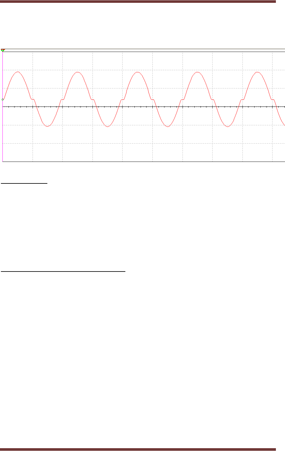
ECA Lab manual
Dept of ECE, Lendi Institute of Engineering and Technology Page 62
RESULT:
VIVA QUESTIONS:
1. What are the conditions of oscillations?
2. Give the formula for frequency of oscillations?
3. What is the total phase shift produce by the RC ladder network?
4. Whether the oscillator is positive feedback or negative feedback?
5. What are the types of oscillators?
6. What is the gain of RC phase shift oscillator?
7. What is the difference between damped oscillations undamped oscillations?
8. What are the applications of RC oscillations?
9. How many resistors and capacitors are used in RC phase shift network
10. How the Barkhausen criterion is satisfied in RC phase shift oscillator

ECA Lab manual
Dept of ECE, Lendi Institute of Engineering and Technology Page 63
3. CLASS B COMPLEMENTARY SYMMETRY AMPLIFIER
AIM: To observe the input and output waveforms and to calculate the efficiency of Class B
Complimentary symmetry power amplifier.
EQUIPMENT REQUIRED: PSPICE Simulation Software
CIRCUIT DIAGRAM:
THEORY:
An amplifying system consists of several stages in cascade. The input and the
intermediate stages amplify small signal excitations to a value large enough to drive the final
device .The out put stage feeds the final device .The output stage feeds a transducer such as a
CRO,loudspeaker or servomotor. Thus the final stage must be capable of delivering a large
voltage or current or appreciable amount of power. This requires an amplifier which is
referred as a power amplifier
In class B complimentary symmetry class _B amplifier one n-p-n and p-n-p is used. Hence
the circuit is called class-B complimentary symmetry amplifier. This circuit ifis transformer
less circuit .But with common emitter configuration it becomes power transfer without output
impedance for maximum power transfer without an output transformers. Hence the matched
pair of complementary transistors are used in common collector configuration This is because
in common collector configuration has lowest output impedance and hence the impedance
matching is possible.

ECA Lab manual
Dept of ECE, Lendi Institute of Engineering and Technology Page 64
PROCEDURE:
1. Enter in to the Pspice software.
2. Customize the screen and then draw the circuit on the screen .
3. Start the simulation and observe the input and output waveforms.
MODEL GRAPHS:
RESULT:.
VIVA QUESTIONS
1. What is the efficiency of Class B complimentary symmetry power amplifier?
2. What are the advantages of Class B complimentary symmetry power amplifier?
3. What are the disadvantages in Class B push pull power amplifier?

ECA Lab manual
Dept of ECE, Lendi Institute of Engineering and Technology Page 65
4. WEIN BRIDGE OSCILLATOR
AIM: To study and calculate frequency of Wein Bridge Oscillator.
APPARATUS:
Pspice software
CIRCUITDIAGRAM:
THEORY:
The wein bridge oscillator is a standard circuit for generating low frequencies in the
range of 10 Hz to about 1MHz.The method used for getting +ve feedback in wein bridge
oscillator is to use two stages of an RC-coupled amplifier. Since one stage of the RC-
coupled amplifier introduces a phase shift of 180 deg, two stages will introduces a phase shift
of 360 deg. At the frequency of oscillations f the +ve feedback network shown in fig makes
the input & output in the phase. The frequency of oscillations is given as
f =1/2π√R
1
C
1
R
2
C
2
In addition to the positive feedback

ECA Lab manual
Dept of ECE, Lendi Institute of Engineering and Technology Page 66
PROCEDURE:
1. Enter in to the Pspice software.
2. Customize the screen and then draw the circuit on the screen .
3. Start the simulation and observe the input and output waveforms.
MODEL WAVE FORM:
RESULT:
VIVA QUESTIONS:
1. Give the formula for frequency of oscillations?
2. What is the condition for wien bridge oscillator to generate oscillations?
3. What is the total phase shift provided by the oscillator?
4. What is the function of lead-lag network in Wein bridge oscillator?
5. which type of feedback is used in Wein bridge oscillator
6. What is gain of Wein bridge oscillator?
7. what are the application of Wein bridge oscillator
8. What is the condition for oscillations?
9. What is the difference between damped oscillations undamped Oscillations?

ECA Lab manual
Dept of ECE, Lendi Institute of Engineering and Technology Page 67
5. CLASSA POWER AMPLIFIER
AIM: To
o
b
s
e
r
ve the input and outp
u
t
w
ave
f
o
r
m
s
and to calculate the e
ff
iciency o
f
CL
ASS
A
P
o
w
e
r
A
mpli
f
ie
r
.
EQUIPMENT REQUIRED: PSPICE Simulation Software
CIRCUIT DIAGRAM:
THEORY:
The ampli
f
ie
r
i
s
s
aid to be cla
ss
A
po
w
e
r
ampli
f
ie
r
i
f
the q point and the input
s
ignal a
r
e
s
elected
s
uch that the output
s
ignal i
s
obtained
f
o
r
a
f
ull input cycle .
F
o
r
thi
s
cla
ss
the po
s
ition o
f
q point i
s
app
r
oximately y at the mid point o
f
the load line.
F
o
r
all the value
s
o
f
input
s
ignal the t
r
an
s
i
s
to
r
r
emain
s
in the active
r
egion and
neve
r
enti
r
e into the cuto
ff
o
r
s
atu
r
ation
r
egion. The collecto
r
cu
rr
ent
f
lo
ws
f
o
r
3600
(
li
f
e cycle
)
o
f
the input
s
ignal in othe
r
w
o
r
d
s
the angle o
f
the collecto
r
cu
rr
ent
f
lo
w
i
s
3600 the claa a ampli
f
ie
rs
o
r
f
u
r
the
rs
cla
ss
i
f
ied a
s
di
r
ectly coupled and t
r
an
sf
o
r
me
r
coupled and t
r
an
sf
o
r
me
r
coupled ampli
f
ie
rs
in di
r
ectly coupled type .The load i
s
di
r
ectly connected in the collecto
r
ci
r
cuit
w
hile in the t
r
an
sf
o
r
me
r
coupled type,
the l
o
ad i
s
coupled to the collecto
r
u
s
ing the t
r
an
sf
o
r
me
r
.
A
dvantage
s
:
1.
D
i
s
to
r
tion analy
s
i
s
i
s
ve
r
y impo
r
tant
2.
I
t ampli
f
ie
s
audio
fr
equency
s
ignal
s
f
aith
f
ully hence they a
r
e called a
s
audio ampli
f
ie
rs
D
i
s
advantage
s
:
1.
H
pa
r
amete
r
analy
s
i
s
i
s
not applicable

ECA Lab manual
Dept of ECE, Lendi Institute of Engineering and Technology Page 68
2.
D
ue to la
r
ge po
w
e
r
handling the t
r
an
s
i
s
to
r
i
s
u
s
ed po
w
e
r
t
r
an
s
i
s
to
r
w
hich i
s
la
r
ge in
s
ize and having la
r
ge po
w
e
r
r
ating
PROCEDURE:
1. Enter in to the Pspice software.
2. Customize the screen and then draw the circuit on the screen .
3. Start the simulation and observe the input and output waveforms.
GRAPH:
I/P
O/P:
FREQUENCY RESPONSE:

ECA Lab manual
Dept of ECE, Lendi Institute of Engineering and Technology Page 69
RESULT:.
VIVA QUESTIONS:
1.On which criteria based the power amplifiers are classified?
2.what is the operating point of class-A power ampliier?
3.what is meant by efficiency?
4.howmuch efficiency will b obtained in classs-A power amplifier?
5. what are the applications of power amplifier?

ECA Lab manual
Dept of ECE, Lendi Institute of Engineering and Technology Page 70
6.SINGLE TUNED VOLTAGE AMPLIFIER
AIM: To study single tuned voltage Amplifier and to calculate
1. Resonant Frequency.
2. Q factor.
3. Bandwidth and
4. Impedance
APPARATUS: Pspice software
CIRCUIT DIAGRAM:
THEORY:
It is usually required to use a number of tuned amplifier stages in cascade in order to
obtain large overall gain. These cascade tuned amplifiers may be put into the following
three categories:
1. Single tuned amplifiers.
2. Double tuned amplifiers.
3. Stagger-tuned amplifiers.
Single tuned amplifiers use one parallel tuned circuit as the load impedance in each stage and
all these tuned circuits in different stages are tuned to the same frequency.Double tuned
amplifier uses two inductively coupled tuned circuits per stage, both the tuned circuits being
tuned to the same frequency.Staggered tuned amplifier uses a number of single tuned stages
in cascade, the successive tuned circuits being tuned to slightly different frequencies.
Single tuned amplifiers may again be put into following two categories:
a) Capacitance coupled single tuned amplifiers and
b) Transformer coupled or inductively coupled single tuned amplifiers
RESONANT FREQUENCY:
Depending upon the frequency of the source voltage Vs, the circuits may behave either as
inductive or capacitive. However, at a particular frequency when the inductive reactance Xl
equals the capacitive reactance Xc, then the circuit behaves as a purely resistive circuit. This

ECA Lab manual
Dept of ECE, Lendi Institute of Engineering and Technology Page 71
phenomenon is called resonance: and the corresponding frequency is called resonant
frequency. The resonant frequency (fr) can be found by equating the two reactance values.
PROCEDURE:
1. Enter in to the Pspice software.
2. Customize the screen and then draw the circuit on the screen .
3. Start the simulation and observe the input and output waveforms.
GRAPH:

ECA Lab manual
Dept of ECE, Lendi Institute of Engineering and Technology Page 72
RESULT:.
VIVA QUESTIONS:
1. What are tuned amplifiers?
2. What is tuning?
3. Explain how the tuned amplifiers work?

ECA Lab manual
Dept of ECE, Lendi Institute of Engineering and Technology Page 73
8. CLASS -A POWER AMPLIFIER(TRANSFORMER COUPLED)
AIM: To
o
b
s
e
r
ve the input and outp
u
t
w
ave
f
o
r
m
s
and to calculate the e
ff
iciency o
f
CL
ASS
A
P
o
w
e
r
A
mpli
f
ie
r
.
EQUIPMENT REQUIRED: Pspice software
CIRCUIT DIAGRAM:
THEORY:
The ampli
f
ie
r
i
s
s
aid to be cla
ss
A
po
w
e
r
ampli
f
ie
r
i
f
the q point and the input
s
ignal a
r
e
s
elected
s
uch that the output
s
ignal i
s
obtained
f
o
r
a
f
ull input cycle .
F
o
r
thi
s
cla
ss
the po
s
ition o
f
q point i
s
app
r
oximately y at the mid point o
f
the load line.
F
o
r
all the value
s
o
f
input
s
ignal the t
r
an
s
i
s
to
r
r
emain
s
in the active
r
egion and
neve
r
enti
r
e into the cuto
ff
o
r
s
atu
r
ation
r
egion. The collecto
r
cu
rr
ent
f
lo
ws
f
o
r
3600
(
li
f
e cycle
)
o
f
the input
s
ignal in othe
r
w
o
r
d
s
the angle o
f
the collecto
r
cu
rr
ent
f
lo
w
i
s
3600 the claa a ampli
f
ie
rs
o
r
f
u
r
the
rs
cla
ss
i
f
ied a
s
di
r
ectly coupled and t
r
an
sf
o
r
me
r
coupled and t
r
an
sf
o
r
me
r
coupled ampli
f
ie
rs
in di
r
ectly coupled type .The load i
s
di
r
ectly connected in the collecto
r
ci
r
cuit
w
hile in the t
r
an
sf
o
r
me
r
coupled type,
the l
o
ad i
s
coupled to the collecto
r
u
s
ing the t
r
an
sf
o
r
me
r
.
A
dvantage
s
:
1.
D
i
s
to
r
tion analy
s
i
s
i
s
ve
r
y impo
r
tant
2.
I
t ampli
f
ie
s
audio
fr
equency
s
ignal
s
f
aith
f
ully hence they a
r
e called a
s
audio ampli
f
ie
rs
D
i
s
advantage
s
:

ECA Lab manual
Dept of ECE, Lendi Institute of Engineering and Technology Page 74
1.
H
pa
r
amete
r
analy
s
i
s
i
s
not applicable
2.
D
ue to la
r
ge po
w
e
r
handling the t
r
an
s
i
s
to
r
i
s
u
s
ed po
w
e
r
t
r
an
s
i
s
to
r
w
hich i
s
la
r
ge in
s
ize and having la
r
ge po
w
e
r
r
ating
PROCEDURE:
1. Enter in to the Pspice software.
2. Customize the screen and then draw the circuit on the screen .
3. Start the simulation and observe the input and output waveforms.
GRAPH:
I/P
O/P:

ECA Lab manual
Dept of ECE, Lendi Institute of Engineering and Technology Page 75
RESULT:
VIVA QUESTIONS:
1.On which criteria based the power amplifiers are classified?
2.what is the operating point of class-A power ampliier?
3.what is meant by efficiency?
4.how much efficiency will b obtained in classs-A power amplifier?
5. what are the applications of power amplifier?

ECA Lab manual
Dept of ECE, Lendi Institute of Engineering and Technology Page 76

ECA Lab manual
Dept of ECE, Lendi Institute of Engineering and Technology Page 77
8.VOLTAGE-SERIES FEEDBACK AMPLIFIER
AIM: To study the effect of voltage series feedback and Gain of the Amplifier.
APPARATUS: Pspice Software
CIRCUIT DIAGRAM:
THEORY:
When any increase in the output signal results into the input in such a way as to cause
the decrease in the output signal, the amplifier is said to have negative feedback. The
advantages of providing negative feedback are that the transfer gain of the amplifier with
feedback can be stablised against varations in the hybrid parameteresof the transistor or the
parameters of the other active devices used in the circuit. The most advantage of the negative
feedback is that by propere use of this , there is significant improvement in the frequency
respponse and in the linearity of the operation of the amplifier.This disadvantage of the
negative feedback is that the voltage gain is decreased.
In Voltage-Series feedback , the input impedance of the amplifier is decreased and the
output impedance is increased.Noise and distortionsare reduced cosiderably.
PROCEDURE:
1. Enter in to the Pspice software.
2. Customize the screen and then draw the circuit on the screen .
3. Start the simulation and observe the input and output waveforms.

ECA Lab manual
Dept of ECE, Lendi Institute of Engineering and Technology Page 78
GRAPH:
o/p:
Frequency response:

ECA Lab manual
Dept of ECE, Lendi Institute of Engineering and Technology Page 79
Result:
Viva voice:
1. what is meant by feed back?
2. what are the types of feed back?
3. why we are using negative feed back in feedback amplifiers?
4.what are the different types of feedback amplifiers?

ECA Lab manual
Dept of ECE, Lendi Institute of Engineering and Technology Page 80
10. CURRENT SHUNT FEEDBACK AMPLIFIER
AIM: To observe the performance of a current shunt feedback amplifier and obtain its
bandwidth.
EQUIPMENT RQUIRED: Pspice Software
THEORY:
Current shunt feedback circuit shows two transistor in cascade with feedback from the
second emitter to the first base through the resistor R
F
. we verify that this connection
produces negative feedback. The voltage V
i2
is much larger than V
i1
because of the voltage
gain of Q
1
. Also V
i2
is 180
0
out of phase with V
i1
. Because of emitter follower action V
e2
is
only slightly smaller than V
i2
, and these voltages are in phase. Hence V
e2
is larger in
magnitude than V
i1
and is 180
0
out of phase with V
i1
. If the input signal increases so that I
S
increases, If also increases, and I
i
= I
S
- I
f
is smaller than it would be their were no
feedback. This action is characteristics of negative feedback.
CIRCUIT DIAGRAM:
PROCEDURE:
1. Enter in to the Pspice software.
2. Customize the screen and then draw the circuit on the screen .
3. Start the simulation and observe the input and output waveforms.

ECA Lab manual
Dept of ECE, Lendi Institute of Engineering and Technology Page 81
GRAPHS:
RESULT:
CONCLUSIONS:
Conclusions can be drawn on comparing the voltage gain of the amplifier with and
without feedback, bandwidth obtained from the frequency response plot.
VIVA QUESTIONS:
5. What is the relationship between the transfer gain with feedback A
f
and that without feedback
A.
6. Define negative feedback.
7. Define the amount of feedback in decibels.
8. State the three fundamental assumptions which are made in order that the expression A
f
=
A/(1+A
) be satisfy exactly.
A
V
max.
Gain in dB
Frequency
-3 dB point.
f
L
f
H
Bandwidth = f
H
-
f
L

ECA Lab manual
Dept of ECE, Lendi Institute of Engineering and Technology Page 82
10.CLASS B PUSH PULL POWER AMPLIFIER
AIM: To observe the input and output waveforms and to calculate the efficiency of Class B
Complimentary symmetry power amplifier.
EQUIPMENT REQUIRED: Pspice software
CIRCUIT DIAGRAM:
THEORY:
An amplifying system consists of several stages in cascade. The input and the intermediate stages
amplify small signal excitations to a value large enough to drive the final device .The out put
stage feeds the final device .The output stage feeds a transducer such as a CRO,loudspeaker or
servomotor. Thus the final stage must be capable of delivering a large voltage or current or
appreciable amount of power. This requires an amplifier which is referred as a power amplifier
In class B complimentary symmetry class _B amplifier one n-p-n and p-n-p is used. Hence the
circuit is called class-B complimentary symmetry amplifier. This circuit ifis transformer less
circuit .But with common emitter configuration it becomes power transfer without output
impedance for maximum power transfer without an output transformers. Hence the matched pair
of complementary transistors are used in common collector configuration This is because in
common collector configuration has lowest output impedance and hence the impedance matching
is possible.
PROCEDURE:
1.conncet the circuit s per the circuit diagram
2.apply 4v p-p with 1KHZ frequency using function generator
3.observe the output in CRO .
4.note the cross over distortion in output.(outputVp-p)

ECA Lab manual
Dept of ECE, Lendi Institute of Engineering and Technology Page 83
5.remove the collector connection and put ammeter.
6.note the Idc value in the ammeter.
7.using Pdc and Pac formulas find the efficiency.
GRAPHS:
RESULT:
VIVA QUESTIONS:
1.In classB power amplifiers why crossover distortion will be occurred?
2.what are he different methods to eliminate distortion?
3..howmuch efficiency will b obtained in classs-B power amplifier?
4.where is the location of operating point in class-B power amplifier?

ECA Lab manual
Dept of ECE, Lendi Institute of Engineering and Technology Page 84
PROJECTS RELATED TO LAB
Water Level Indicator Circuit Diagram:
Water Level Indicator Project Block Diagram:

ECA Lab manual
Dept of ECE, Lendi Institute of Engineering and Technology Page 85
Automatic Room Light Switch Circuit Diagram:
Block Diagram of Boolean Algebra Calculator:

ECA Lab manual
Dept of ECE, Lendi Institute of Engineering and Technology Page 86
Boolean Algebra Calculator Circuit Diagram:
Simple Mobile Jammer Circuit Diagram:

ECA Lab manual
Dept of ECE, Lendi Institute of Engineering and Technology Page 87
Block Diagram of Metal Detector:
Circuit Diagram of Metal Detector:
