
Analog circuits lab manual 18ECL48
Dept.of ECE. VSMSRKIT,Nipani
VSM’s
Somashekhar R Kothiwale Institute of
Technology, Nipani-591237
Department of Electronics &
Communication Engg
ANALOG CIRCUITS LAB
18ECL48
By
Prof.Govind M R

Analog circuits lab manual 18ECL48
Dept.of ECE. VSMSRKIT,Nipani
Laboratory Code
18ECL48
CIE Marks
40
Number of Lecture
Hours/Week
02 Hr Tutorial (Instructions) + 02 Hours
Laboratory
SEE Marks
60
RBT Level
L1, L2, L3
Exam Hours
03
ANALOG CIRCUITS LABORATORY
CREDITS – 02 Course Learning Objectives: This laboratory course enables students to
• Understand the circuit configurations and connectivity of BJT and FET Amplifiers and Study
of frequency response
• Design and test of analog circuits using OPAMPs
• Understand the feedback configurations of transistor and OPAMP circuits
• Use of circuit simulation for the analysis of electronic circuits.
Laboratory Experiments (Syllabus)
PART A : Hardware Experiments
1. Design and setup the Common Source JFET/MOSFET amplifier and plot the frequency
response.
2. Design and set up the BJT common emitter voltage amplifier with and without feedback and
determine the gain- bandwidth product, input and output impedances.
3. Design and set-up BJT/FET i) Colpitt‟s Oscillator, and ii) Crystal Oscillator
4. Design active second order Butterworth low pass and high pass filters.
5. Design Adder, Integrator and Differentiator circuits using Op-Amp
6. Test a comparator circuit and design a Schmitt trigger for the given UTP and LTP values and
obtain the hysteresis.
7. Design 4 bit R – 2R Op-Amp Digital to Analog Converter (i) using 4 bit binary input from
toggle switches and (ii) by generating digital inputs using mod-16 counter.
8. Design Monostable and a stable Multivibrator using 555 Timer.
Analog circuits lab manual 18ECL48
Dept.of ECE. VSMSRKIT,Nipani
PART-B : Simulation using EDA software (EDWinXP, PSpice, MultiSim, Proteus,
CircuitLab or any other equivalent tool can be used)
1. RC Phase shift oscillator and Hartley oscillator
2. Narrow Band-pass Filter and Narrow band-reject filter
3. Precision Half and full wave rectifier
4. Monostable and Astable Multivibrator using 555 Timer.
Course Outcomes: On the completion of this laboratory course, the students will be able to:
CO1: 18ECL48.1 ;Design analog circuits using BJT/FETs and evaluate their performance
characteristics.
CO2: 18ECL48.2 ;Design analog circuits using OPAMPs for different applications
CO2: 18ECL48.3;Simulate and analyze analog circuits that uses ICs for different electronic
applications.
Conduct of Practical Examination:
• All laboratory experiments are to be included for practical examination.
• Students are allowed to pick one experiment from the lot.
• Strictly follow the instructions as printed on the cover page of answer script for breakup of
marks.
• Change of experiment is allowed only once and Marks allotted to the procedure part to be made
zero.
Reference Books: 1. David A Bell, “Fundamentals of Electronic Devices and Circuits Lab
Manual, 5th Edition, 2009, Oxford university press.

Analog circuits lab manual 18ECL48
Dept.of ECE. VSMSRKIT,Nipani
Circuit diagram
Fig:CS Amplifier using voltage divider bias
Design
Selection of FET: Select BFW10 or BFW11
DC bias conditions
V
DD
=12V, V
GS
= -1V, V
RS
=20% of V
DD
=2.4 V
V
RD
=V
DS
=45% of V
DD
=5.4V.
Design of R
D
Given, V
RD
=I
D
R
D
=5.4V. From this we get R
D
=2.7 k. Use R
D
=2.7k
Design of R
S
R
S
=
=
But I
D
=I
S
=2 mA
And V
RS
=1.2V
Substituting these values we get R
s
=600Ω
Use R
S
=680Ω
Design of R1 and R2
V
R2
=V
GS
+V
RS
=1.2V
Also, V
R2
=V
DD
×
2
1+2
Use large value of R1 to ensure zero gate current.

Analog circuits lab manual 18ECL48
Dept.of ECE. VSMSRKIT,Nipani
1. Design and setup the Common Source JFET/MOSFET amplifier and plot
the frequency response.
Aim: To design, setup and plot the frequency response of a common JFET amplifier
Apparatus Required
Theory:
Junction Field effect Transistor(JFET) is a unipolar voltage controlled device. The drain current
is controlled by the voltage applied at the gate. Like BJT, JFET amplifiers can also be setup in
three configurations namely , common drain, common source and common gate. The common
source configuration is similar to common emitter configuration of BJTs. JFETs can be biased as
voltage divider bias or self-bias.
CS amplifier using voltage divider bias
The voltage divider bias is used to maintain stable bias voltage at the FET terminals independent
of drain current. A voltage divider bias can be obtained by a small modification on the self bias
circuit. Refer to the circuit diagram shown in figure. Two high value resistors R1 and R2 establishes
potential divider bias. In order to maintain a negative voltage across gate and source terminals R1 and
R2 are selected in such a way that potential at the source is more than that at gate.
Sl.
No.
Particulars
Range
Quantity
1.
JFET
-
1 each
2.
Resistors & Capacitors
As per design
-
3.
Multi meter
-
01
4.
DCB
-
02
5.
Breadboard and connecting wires
-
-

Analog circuits lab manual 18ECL48
Dept.of ECE. VSMSRKIT,Nipani
Take R1=1MΩ
Substituting the known values in the expression for V
R2
, we get
R2=13.2k . Use R2=12k
Design of R
L
Gain of CS amplifier A=15=g
m
(R
D
||R
L
)
Since required A=15, we get R
L
=4.7k.
Design of coupling capacitors C
C1
and C
C2
We know ,
C
C1
=
1
2
×
Substituting f
L
=100Hz and R
g
=1MΩ ,we get
C
C1
=1.59 pF
Take C
C1
=C
C2
=1 pF.
Design of bypass capacitor C
S
Take X
CS
=R
S
/10 at 100Hz to bypass this frequency.
Then
X
CS
≤100Ω
So
C
S
≥
1
2
×100
=16µF
Use C
S
=22µF.
Graph
log f
Bandwidth
log f
L
log F
H
Gain in dB
M
1
dB
M
1
-3 dB
3dB
Analog circuits lab manual 18ECL48
Dept.of ECE. VSMSRKIT,Nipani
Procedure
1. Check and verify the dc bias conditions without connecting capacitors and ac input signal.
2. Connect the capacitors in the circuit. Apply a 100 mV peak to peak sinusoidal signal from
the function generator to the circuit input. Observe the input and output waveforms on the
CRO screen simultaneously.
3. Keep the input voltage constant at 200 mV, vary the frequency of the input signal from 0 to 1
MHz or highest frequency available in the generator. Measure the output peak-to-peak
voltage corresponding to different frequencies and enter it in tabular column.
4. Plot the frequency response characteristics on a semilog sheet with gain in dB on y-axis and f
requecny on x-axis. Mark l
fL
and f
H
corresponding to 3 dB points.
5. Calculate the bandwidth of the amplifier using the expression BW= f
H
-f
L
.
Result
Bandwidth=………Hz
Viva voce questions
1. Define ohmic, saturation and pinch off regions of a JFET.
2. Why is the FET very suitable for instrumentation applications?
3. Differentiate FET and BJT amplifiers
4. Why is the bandwidth of FET amplifiers high?

Analog circuits lab manual 18ECL48
Dept.of ECE. VSMSRKIT,Nipani
Observation
Input voltage = volts
f(Hz)
V
o
(volts, V
PP
)
Gain=
Gain in dB=20log(
)

Analog circuits lab manual 18ECL48
Dept.of ECE. VSMSRKIT,Nipani
Circuit diagram
Fig : Circuit diagram of Common Emitter Amplifier using BJT
Design
Given, V
CE
= 5 V and I
C
= 2 mA Assume = 100
V
CC
= 2V
CE
= 2 X 5 = 10 V
Let V
RE
= 10% V
CC
= 1 V
R
E
= V
RE
/ ( I
C
+ I
B
)
I
B
= I
C
/ = 2 mA / 100 = 20 A
R
E
= 1 / ( 2 m + 20 ) = 495
Choose R
E
= 470
Apply KVL to collector loop
V
CC
– I
C
R
C
– V
CE
– V
E
= 0
R
C
= ( V
CC
– V
CE
– V
E
) / I
C
= ( 10 – 5 – 1 ) / 2 m
R
C
= 2 k Choose R
C
= 1.8 k
Let I
R1
= 10 I
B
= 10 X 20 A = 200 A
V
R2
= V
BE
+ V
E
= 0.6 + 1 = 1.6 V( Since transistor is silicon make V
BE
= 0.6 V )
R
2
= V
R2
/ ( I
R1
– I
B
) = 1.6 / ( 200 A - 20 A )
R
2
= 8.8 k Choose R
2
= 8.2 k

Analog circuits lab manual 18ECL48
Dept.of ECE. VSMSRKIT,Nipani
2. Design and set up the BJT common emitter voltage amplifier with and without feedback
and determine the gain- bandwidth product, input and output impedances.
Aim : To design and setup a common emitter (CE) amplifier under voltage divider bias with
and without feedback and to determine the gain-bandwidth product from its frequency response.
Components and equipment required
Sl.
No.
Particulars
Range
Quantity
1.
Transistor SL 100
-
01
2.
Resistors & Capacitors
As per design
-
3.
CRO Probes
-
3 Set
4.
Multi meter
-
01
5.
DRB
-
01
6.
Spring board and connecting wires
-
-
Theory:An amplifier is a circuit which increases the voltage, current or power level of i/p
signal where the frequency is maintained constant from o/p to i/p signal. The common emitter
amplifier is basically a current amplifier ( I
C
= I
B
) where I
B
is input current and IC is output
current and is a non unity value, in turn it provides voltage amplification. The ratio of
collector current to base current is noted as the current amplification factor and is denoted as
‘’i.e.[ = I
C
/I
B
], is very large.
In RC coupled CE amplifier R
1
, R
2
and R
C
are selected in such a way that transistor
operates in active region and the operating point will be in the middle of active region. R
E
is used
for stabilization of operating point. Coupling capacitors C
C1
and C
C2
are used to block dc current
flow through load and the source. The emitter by-pass capacitor C
E
is connected to avoid
negative feedback. Input signal increases base current and the collector current increases by a
factor . [i.e., I
c
= I
b
]. Hence output voltage is large compared to input voltage which is known
as amplification. An amplifier in which resistance-capacitance coupling is employed between
stages and at the input and an output point of the circuit is known as RC coupled amplifier. A
capacitor provides a path for signal currents between stages, with resistors connected from each
side of the capacitor to the power supply or to ground.
Procedure:
6. Check and verify the dc bias conditions without connecting capacitors and ac input signal.
7. Connect the capacitors in the circuit. Apply a 100 mV peak to peak sinusoidal signal from
the function generator to the circuit input. Observe the input and output waveforms on the
CRO screen simultaneously.
8. Keep the input voltage constant at 200 mV, vary the frequency of the input signal from 0 to 1
MHz or highest frequency available in the generator. Measure the output peak-to-peak
voltage corresponding to different frequencies and enter it in tabular column.
9. Plot the frequency response characteristics on a semilog sheet with gain in dB on y-axis and f
requecny on x-axis. Mark l
fL
and f
H
corresponding to 3 dB points.
10. Calculate the bandwidth of the amplifier using the expression BW= f
H
-f
L
.

Analog circuits lab manual 18ECL48
Dept.of ECE. VSMSRKIT,Nipani
R
1
= ( V
CC
– V
R2
) / I
R1
= ( 10 – 1.6 ) / 200 A
R
1
= 42 K Choose R
1
= 47 k
X
CE
<< R
E ,
X
CE
= R
E
/ 10
1 / ( 2 f C
E
) = 470 / 10 Let f = 100 Hz
C
E
= 33 F Choose C
E
= 47 F
Choose C
C1
= C
C2
= 0.1 F
Observations ; Table: CE amplifier without feedback
Input voltage = volts
f in Hz
Vo in Volt
A
V
= Vo / V
i
Gain in dB = 20*log A
V
Circuit diagram to find input impedance(Z
i
):
Circuit diagram to find output impedance(Z
o
):

Analog circuits lab manual 18ECL48
Dept.of ECE. VSMSRKIT,Nipani
11. Determine the mid-band gain from the graph plotted.
12. Calculate the gain-bandwidth product.
13. Remove the emitter bypass capacitor CE from the circuit and repeat the steps 3 to 6 and
observe that the bandwidth increases and gain decreases in the absence of C
E
.
To find the input impedance ( Zi ) :
1. Connections are made as shown in the diagram.
2. Keeping the DRB in its minimum position, apply input signal at mid band frequency (say
10 kHz) and adjust the amplitude of the input signal to get distortion less output. Note
down the output amplitude.
3. Vary the DRB until the output amplitude becomes half of its previous value. The
corresponding DRB value gives the input impedance.
To find the output impedance ( Zo ) :
1.Connections are made as shown in the diagram.
2.Keeping the DRB in its maximum position, apply input signal at mid band frequency
(say10kHz) and adjust the amplitude of the input signal to get distortionless output. Note
down the output amplitude.
3.Vary the DRB until the output amplitude becomes half of its previous value. The corresponding
DRB value gives the output impedance.
Ideal Graph
Frequency response of RC coupled amplifier with and without feedback

Analog circuits lab manual 18ECL48
Dept.of ECE. VSMSRKIT,Nipani
Table: CE amplifier with feedback. Input voltage = volts
f in Hz
Vo in Volt
A
V
= Vo / V
i
Gain in dB = 20*log A
V
Result
The CE amplifier with voltage divider bias circuit with and without feedback is designed and
frequency response is drawn, bandwidth is calculated from the frequency curve.
Without feedback:
Gain = ………dB
Bandwidth = ……….dB
Gain-Bandwidth product = ………..dB
Input impedance (Z
i
) = ____________, Output Impedance (Zo) = __________
Analog circuits lab manual 18ECL48
Dept.of ECE. VSMSRKIT,Nipani
With feedback:
Gain = ……….dB
Bandwidth = ………..dB
Gain-Bandwidth product = ………..dB
Input impedance (Z
i
) = ____________, Output Impedance (Zo) = __________
Viva voce questions
1. Define gain of the amplifier
2. What are the functions of the three resistances R
1
, R
2
, R
E
?
3. What are the functions of the capacitances C
E
and C
C
?
4. explain the Thevenin‟s model of the voltage divider bias
network
5. How can a transistor be operated as a switch?
6. Which configuration of a transistor is preferred when a
transistor is used as a switch and why?
7. What is quiescent point?
8. What is load line?
9. Why is the Q – point always at the centre of the load line?
10. Why are the coupling capacitors used?
11. Why are there 2 circuits namely the biasing circuit and
amplifier circuit?
12. Explain why the frequency response is as it is shown?
13. Explain why only a 3dB bandwidth is chosen?
14. What is early effect?
15. Compare FET with BJT

Analog circuits lab manual 18ECL48
Dept.of ECE. VSMSRKIT,Nipani
Circuit Diagram:
Given V
CE
=6V and Ic=2mA ,Aussume β=200.
Vcc=2* V
CE
= 12v, Let V
RE
=10%Vcc=1.2v. R
E
= V
RE/ (I c
+I
b
), I
b
=Ic/ β, I
b=
2mA/200=10µA
R
E
=1.2/(2mA+10µA)=497.4Ω, Choose=470 Ω.
Apply KVL to collector loop
V
CC
-I
C
R
C
-V
CE
-V
E=0 .
R
c=
(V
CC
-VCE-V
E ) /
I
C
R
C=(12-6-1.2) /2mA = 2.4K
Ω ,choose 2.2k Ω
Let I
R1
=10*I
B =
10
*
10µA=100µA.
V
R2
=V
BE
+V
E
= 0.6+1.2=1.8V ( For silicon transistor V
BE
=0.6v)
R
2
= V
R1
/ (I
R1
-I
B
) =1.8 /(100µA - 10µA) =20K Ω. Choose R2= 18k Ω.
R
1
= ( V
cc-
V
R2
/ I
R1
) = (12- 1.8)/ 100µA = 102K Ω. Choose R
1
= 82k Ω.
X
CE <<
R
E ,
Let
X
CE =
R
E/10, 1 /
2fC
E =
470/10 , Let f=100hz. C
E=
33µF, Choose C
E
=47µF.
Take C
C1
=C
C2
=0.01 µF

Analog circuits lab manual 18ECL48
Dept.of ECE. VSMSRKIT,Nipani
3. Design and set-up BJT/FET i) Colpitts Oscillator, and ii) Crystal Oscillator
Aim:To design and set up the following tuned oscillator circuits using BJT ,and calculate frequency of
output waveform. 1.Colpitts Oscillator. 2.Crystal Oscillator
Apparatus Required:
Sl.
No.
Particulars
Range
Quantity
1.
BJT SL100
-
01
2.
Resistors & Capacitors
As per design
-
3.
Crystal
As per design
01
4.
CRO Probes
-
3 Set
5.
Multi meter
-
01
6.
DCB, DIB
-
2 each
7.
Spring board and connecting wires
-
-
Theory: .A Colpitt’s oscillator, named after its inventor Edwin H. Colpitt‟s, is one of a number
of designs for electronic oscillator circuits using the combination of an inductance (L) with a
capacitor (C) for frequency determination, thus also called LC oscillator. One of the key features
of this type of oscillator is its simplicity (needs only a single inductor) and robustness. A
Colpitt‟s oscillator is the electrical dual of a Hartley oscillator. Fig. 1 shows the basic Colpitt‟s
circuit, where two capacitors and one inductor determine the frequency of oscillation. The
feedback needed for oscillation is taken from a voltage divider made by the two capacitors, The
basic CE amplifier provides 180 phase shift and the feed back network provides the remaining
180 phase shift so that the overall phase shift is 360 to satisfy the Barkhausen criteria. The
Barkhausen criteria states that in a positive feedback amplifier to obtain sustained oscillations,
the overall loop gain must be unity ( 1 ) and the overall phase shift must be 0 or 360.
When the power supply is switched on, due to random motion of electrons in passive
components like resistor, capacitor a noise voltage of different frequencies will be developed at
the collector terminal of transistor, out of these the designed frequency signal is fed back to the
amplifier by the feed back network and the process repeats to give suitable oscillation at output
terminal.
Crystal Oscillator In conventional radio frequency oscillation using LC circuits, the frequency
stability is usually poor because of the variations in temperature, humidity, transistor and circuit
parameters, etc. For certain applications such as radio or television transmitters, it is essential that the
frequency of oscillation of master oscillator must be extremely stable. The crystal oscillator is an
excellent solution for this. It provides very high stability and quality factor. A piezoelectric crystal is used
in crystal oscillator as a resonant tank circuit.A crystal acts like a large inductor in series with a small
capacitor. When an alternating voltage is applied across such a crystal, it vibrates at the frequency of the
applied voltage. Conversely it is forced to vibrate, it will generate an alternating voltage. This property is
called piezoelectric effect. The common piezoelectric crystals are Rochelle-salt, Tourmaline and Quartz.
Since quartz is inexpensive and readily available compare to other crystals it is more popular.

Analog circuits lab manual 18ECL48
Dept.of ECE. VSMSRKIT,Nipani
Colpitt’s oscillator: Design of tank circuit: Assume f
o
= 100 kHz
Formula f
o
= 1 / 2 (C
T
. L)
Where C
T
= C
1
. C
2
/ (C
1
+ C
2
)
Barkhausen‟s criterion is A.β = 1
Therefore β = 1/A = C
2
/ C
1
For this circuit, A = 2.4 because gain of the amplifier is 2.4
C
1
= 2.4 · C
2
Assume C
2
= 0.01 µF , therefore C
1
= 0.024 µF, then L = 358.8 µH
Circuit Diagram Output Waveform
Vo
t
T
f
o
= 1 / T Hz
Analog circuits lab manual 18ECL48
Dept.of ECE. VSMSRKIT,Nipani
Procedure:
1. Components / equipment are tested for their good working condition.
2. Connections are made as shown in the diagram
3. The quiescent point of the amplifier is verified for the designed value.
4. Observe the output wave form on CRO and measure the frequency.
5. Verify the frequency with the crystal frequency.
Result:
Crystal Oscillator:
f
o
Theoretical = __________ Hz, f
o
Practical = ____________ Hz
Colpitt’s Oscillator:
f
o
Theoretical = __________ Hz, f
o
Practical = ____________ Hz
Analog circuits lab manual 18ECL48
Dept.of ECE. VSMSRKIT,Nipani
Design:
Given, V
CE
= 6 V and I
C
= 2 mA Assume = 200
V
CC
= 2V
CE
= 2 X 6 = 12V
Let V
RE
= 10% V
CC
= 1.2 V
R
E
= V
RE
/ ( IC + IB )
I
B
= I
C
/ = 2mA / 200 = 10 A
R
E
= 1 / ( 2m + 10 ) = 497.5, Choose R
E
= 470
Apply KVL to collector loop
V
CC
– I
C
R
C
– V
CE
– V
E
= 0
R
C
= ( V
CC
– V
CE
– V
E
) / I
C
= ( 12 – 6– 1.2 ) / 2 m
R
C
= 2.4 k Choose R
C
= 2.2 k
Let I
R1
= 10 I
B
= 10 X 10 A = 100 A
V
R2
= V
BE
+ V
E
= 0.6 + 1.2 = 1.8 V ( Since transistor is silicon make V
BE
= 0.6 V )
R
2
= V
R1
/ ( I
R1
– IB ) = 1.8 / ( 100 A - 10 A ) = 20 K Choose R
2
=18 k
R
1
= ( V
CC
– V
R2
) / IR1 = ( 12 – 1.8 ) / 100 A = 102 K Choose R
1
= 82 k
X
CE
<< R
E
, X
CE
= R
E
/ 10
1 / ( 2 f C
E
) = 470 / 10 Let f = 100 Hz
C
E
= 33 F Choose C
E
= 47 F
Choose C
C1
= 0.01 F, C
C2
= 0.47 F.

Analog circuits lab manual 18ECL48
Dept.of ECE. VSMSRKIT,Nipani
LPF CIRCUIT DIAGRAM:
DESIGN:
LPF for higher cut off frequency F
H
= 2KHz
Input voltage V
in
= 1V
For a 2
nd
order Filter,
F
H
=
1
2
Hz ---------(1)
Assuming C=0.1µF , then
By equation 1,
R= 795.77Ω, choose R= 820Ω
The pass band gain of the filter is
A
F
= 1.586, R
1
= 10KΩ
A
F
= 1 +
RF
R1
R
F
= 5.86KΩ
Choose R
F
=5.6KΩ

Analog circuits lab manual 18ECL48
Dept.of ECE. VSMSRKIT,Nipani
4. Design active second order Butterworth low pass and high pass
filters.
AIM: To draw the frequency response of an second order active LPF and HPF for
a given cut-off frequency.
COMPONENTS REQUIRED:
COMPONENTS
SPECIFICATION
QUANTITY
Resistors
820Ω, 5.6KΩ, 10KΩ,
2,1,1
Capacitors
0.1µF
2
OP-AMP
µA741
1
DC power supply
± 12V
1
Bread board
1
Signal generator
1
CRO
1
BNC
2
Theory:
A low pass filter allows frequency signals only up to a certain break-point fc to pass through, while
suppressing high frequency components as shown in figure.The range of frequencies from 0 to higher
cut-off frequency fc is called passband and the range of frequencies beyond fc is called stopband. The
rate at which the response of a filter falls in the transition band is determined by the order of the filter.
For a second order filter the rolloff factor is -40dB/decade (or -12dB/octave). From the frequency
response as shown in figure .we find that for f<fc , the gain is A. When f =fc, the gain of the filter falls to
0.707 times the maximum gain A. For f>fc , the gain of the filter decreases at a constant rate of -
40dB/decade(or -12dB/octave).
A high pass filter allows only frequencies above a certain breakpoint to pass through and attenuates the
low frequency components as shown in figure. The range of frequencies beyond its lower cut-off
frequency fc is called passband and the range of frequencies from 0 to fc is called stopband. From the
frequency response shown in figure ) we find that for f>fc , the gain is approximately A. At frequency
f=fc , the gain falls to 0.707 times the maximum gain A. For frequency f<fc the gain decreases at a
constant rate of 40dB/decade (or -12dB/octave).

Analog circuits lab manual 18ECL48
Dept.of ECE. VSMSRKIT,Nipani
IDEAL GRAPH:
TABULAR COLUMN:
V
in
= 1V
Sl.
No.
Input signal
frequency in Hz
Output voltage in
Volts
Gain = V
0
/V
in
Gain in dB=
20log (V
0
/V
in
)
1
2
3
4
5
6
7
8
9
10

Analog circuits lab manual 18ECL48
Dept.of ECE. VSMSRKIT,Nipani
PROCEDURE:
1. Connections are made as shown in the fig.
2. Set the input voltage to 1v.
3. By varying the frequency of input from Hz range to KHz range, note the frequency and
the corresponding output voltage across pin 6 of the op amp with respect to the ground.
4. Tabulate the readings in the tabular column.
5. Calculate gain in dB and Plot the frequency response on semi log sheet.
6. Find the cut off frequency using graph and compare it with the theoretical value.
RESULT:
Filter Type
Theoretical cutoff
frequency, Hz
Practical cutoff
Frequency, Hz
Passband gain
LPF
HPF

Analog circuits lab manual 18ECL48
Dept.of ECE. VSMSRKIT,Nipani
HPF CIRCUIT DIAGRAM:
DESIGN:
HPF for lower cut off frequency F
L
= 2KHz
Input voltage V
in
= 1V
For a 2
nd
order Filter,
F
L
=
1
2
Hz ---------(1)
Assuming C=0.1µF , then
By equation 1,
R= 795.77Ω, choose R= 820Ω, IDEAL GRAPH:
TABULAR COLUMN:

Analog circuits lab manual 18ECL48
Dept.of ECE. VSMSRKIT,Nipani
V
in
= 1V
Sl.
No
Input signal
frequency in Hz
Output voltage in
Volts
Gain = V
0
/V
in
Gain in dB=
20log (V
0
/V
in
)
1
2
3
4
5
6
7
8
9
10

Analog circuits lab manual 18ECL48
Dept.of ECE. VSMSRKIT,Nipani
ADDER CIRCUIT DIAGRAM:
R
1
= R
2
= R
3
= R
f
= 100 KΩ
DESIGN
Consider the current flowing through the input resistors are
Then by Kirchoff‟s current law, the current flowing through feedback resistor Rf is given
by the sum of these 3 currents.
This current will flows through the feedback resistor Rf, because the point „K‟ acts
as virtual ground point. So the voltage drop at Rf is given by

Analog circuits lab manual 18ECL48
Dept.of ECE. VSMSRKIT,Nipani
5. Design Adder, Integrator and Differentiator circuits using Op-
Amp
Aim: To design and test Adder, Integrator and Differentiator using Op-Amp
COMPONENTS REQUIRED:
COMPONENTS
SPECIFICATION
QUANTITY
Resistors
As per design
OP-AMP
µA741
1
DC power supply
± 12V
1
Bread board
1
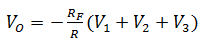
Adder: A two input summing amplifier may be constructed using the inverting mode. The adder
can be obtained by using either non-inverting mode or inverting mode. Here the inverting mode
is used. So the inputs are applied through resistors to the inverting terminal and non-inverting
terminal is grounded. This is called “virtual ground”, i.e. the voltage at that terminal is zero. The
gain of this summing amplifier is 1, any scale factor can be used for the inputs by selecting
proper external resistors.
Integrator: In an integrator circuit, the output voltage is integral of the input signal. The output
voltage of an integrator is given by Vout = -
1
0
.
At low frequencies the gain becomes infinite, so the capacitor is fully charged and behaves like
an open circuit. The gain of an integrator at low frequency can be limited by connecting a
resistor in shunt with capacitor.
Differentiator: In the differentiator circuit the output voltage is the differentiation of the input
voltage. The output voltage of the differentiator is given as. V
OUT
= - R
F
C
.
The input impedance of this circuit decreases with increase in frequency, thereby making
the circuit sensitive to high frequency noise. At high frequencies circuit may become unstable.

Analog circuits lab manual 18ECL48
Dept.of ECE. VSMSRKIT,Nipani
Procedure:
A) Adder
1. Connect the circuit as per the diagram shown in Fig .
2. Apply the supply voltages of ±12V to pin7 and pin4 of IC741 respectively.
3. Apply the inputs V1 and V2 as shown in Fig.
4. Apply two different signals (DC/AC ) to the inputs
5. Vary the input voltages and note down the corresponding output at pin 6 of the IC 741 adder
circuit.
6. Notice that the output is equal to the sum of the two inputs.
Integrator
1. Connect the circuit as per the diagram shown in Fig
2. Apply a square wave/sine input of 4V(p-p) at 1KHz
3. Observe the output at pin 6.
4. Draw input and output waveforms as shown in Fig
Differentiator
1. Connect the circuit as per the diagram shown in Fig
2. Apply a square wave/sine input of 4V(p-p) at 1KHz
3. Observe the output at pin 6
4. Draw the input and output waveforms as shown in Fig
It can be noted that the placement of the capacitor and resistor differs from the integrator
circuit.
-ve sign is due to the op amp connected in inverting mode.

Analog circuits lab manual 18ECL48
Dept.of ECE. VSMSRKIT,Nipani
This circuit is called a summing „amplifier‟ because it can provide gain. By adjusting the
value of Rf the gain can be changed.
Then the output becomes
DIFFERENTIATOR CIRCUIT DIAGRAM:
DESIGN
The node voltage of the operational amplifier at its inverting input terminal is zero, the current, i
flowing through the capacitor will be given as:
I
IN
= I
F
and I
F
= -
The charge on the capacitor equals Capacitance x Voltage across the capacitor
Q = C * V
IN
The rate of change of this charge is:
= C

Analog circuits lab manual 18ECL48
Dept.of ECE. VSMSRKIT,Nipani
but dQ/dt is the capacitor current, i
I
IN
= C
= I
F
i.e, -
= C
from which we have an ideal voltage output for the op-amp differentiator is given as:
V
OUT
= - R
F
C
.
DIFFERENTIATOR OUTPUT WAVEFORM:
DESIGN
The voltage on the plates of a capacitor is equal to the charge on the capacitor divided by its
capacitance giving Q/C. Then the voltage across the capacitor is output Vout therefore: -
Vout = Q/C. If the capacitor is charging and discharging, the rate of charge of voltage across the
capacitor is given as:
V
C
=
, V
C
= V
X
– Vout = 0 – Vout
i.e, -
=
=
1

Analog circuits lab manual 18ECL48
Dept.of ECE. VSMSRKIT,Nipani
But dQ/dt is electric current and since the node voltage of the integrating op-amp at its inverting
input terminal is zero, X = 0, the input current I(in) flowing through the input resistor, Rin is
given as:
I
IN
=
0
=
The current flowing through the feedback capacitor C is given as:
If = C
= C
=
=
Assuming that the input impedance of the op-amp is infinite (ideal op-amp), no current flows
into the op-amp terminal. Therefore, the nodal equation at the inverting input terminal is given
as:
I
IN
= I
f
=
=
i.e,
*
= 1
From which we derive an ideal voltage output for the Op-amp Integrator as:
Vout = -
1
0
= -
To simplify the math‟s a little, this can also be re-written as:
INTEGRATOR CIRCUIT DIAGRAM:

Analog circuits lab manual 18ECL48
Dept.of ECE. VSMSRKIT,Nipani
INTEGRATOR OUTPUT WAVEFORM:
Vout = -
1
Where ω = 2πƒ and the output voltage Vout is a constant 1/RC times the integral of the input
voltage Vin with respect to time. The minus sign ( – ) indicates a 180
o
phase shift because the
input signal is connected directly to the inverting input terminal of the op-amp.
RESULT
Date: Staff-in-charge
CIRCUIT DIAGRAM:

Analog circuits lab manual 18ECL48
Dept.of ECE. VSMSRKIT,Nipani
DESIGN:
Case1:
Given UTP=1V LTP=-1V V
sat
=12V V
ref
=0V
UTP =
Vref R1
( R1 + R2 )
+
Vsat R2
( R1 + R2 )
-----------(1)
LTP =
Vref R1
( R1 + R2 )
-
Vsat R2
( R1 + R2 )
-----------(2)
Subtracting, (1) – (2)
UTP – LTP =
2Vsat R2
( R1 + R2 )
Let R
2
= 1KΩ
1 - (-1) =
2×12×1
(1+1)
R
1
=11 KΩ
6.Test a comparator circuit and design a Schmitt trigger for the given UTP
and LTP values and obtain the hysteresis.

Analog circuits lab manual 18ECL48
Dept.of ECE. VSMSRKIT,Nipani
AIM: To design and test a Schmitt trigger circuit for the values of UTP and LTP, and draw the
hysteresis curve.
COMPONENTS REQUIRED
COMPONENTS
SPECIFICATION
QUANTITY
Resistors
As per design
OP-AMP
µA741
1
DC power supply
± 12V
1
Bread board
1
Signal generator
1
CRO
1
BNC
2
Theory: Schmitt trigger is an electronic circuit with positive feedback which holds the output
level till the input signal to comparator is higher than the threshold. It converts a sinusoidal or
any analog signal to digital signal. It exhibits hysteresis by which the output transition from high
to low and low to high will occur at different thresholds.
It is basically an inverting comparator circuit with a positive feedback. The purpose of the
Schmitt trigger is to convert any regular or irregular shaped input waveform into a square wave
output voltage or pulse. Thus, it can also be called a squaring circuit.
Let us assume that the inverting input voltage has a slight positive value. This will cause a
negative value in the output. This negative voltage is fedback to the non-inverting terminal (+) of
the op-amp through the voltage divider. Thus, the value of the negative voltage that is fedback to
the positive terminal becomes higher. The value of the negative voltage becomes again higher
until the circuit is driven into negative saturation (-Vsat). Now, let us assume that the inverting
input voltage has a slight negative value. This will cause a positive value in the output. This
positive voltage is fedback to the non-inverting terminal (+) of the op-amp through the voltage
divider. Thus, the value of the positive voltage that is fedback to the positive terminal becomes
higher. The value of the positive voltage becomes again higher until the circuit is driven into
positive saturation (+Vsat). This is why the circuit is also named a regenerative comparator
circuit. Schmitt trigger is mostly used to convert a very slowly varying input voltage into an
output having abruptly varying waveform occurring precisely at certain predetermined value of
input voltage. Schmitt trigger may be used for all applications for which a general comparator is
used. Any type of input voltage can be converted into its corresponding square signal wave. The
only condition is that the input signal must have large enough excursion to carry the input
voltage beyond the limits of the hysteresis range. The amplitude of the square wave is
independent of the peak-to-peak value of the input waveform.
Case2:
If V
in
> V
UTP,
THEN V
0
= -V
SAT

Analog circuits lab manual 18ECL48
Dept.of ECE. VSMSRKIT,Nipani
V
in
<V
LTP,
THEN V
0
= +V
SAT
LET UTP= 3V LTP=2V V
sat
=12V
UTP =
Vref R1
( R1 + R2 )
+
Vsat R2
( R1 + R2 )
-----------(1)
LTP =
Vref R1
( R1 + R2 )
-
Vsat R2
( R1 + R2 )
-----------(2)
UTP + LTP =
2Vref R1
( R1 + R2 )
----------(3)
UTP – LTP =
2Vsat R2
( R1 + R2 )
----------(4)
Substituting in (4)
3 - 2 =
2 ×2 ×12
(1+2)
( R
1
+ R
2
) = 24 R
2
R
1
= 23 R
2
Assume R
2
=1KΩ, Therefore R
1
=23 KΩ
Substituting in (3)
V
ref
= 2.6V
Case 3:
LET UTP= 4V LTP=-2V V
sat
= 17 V
UTP =
Vref R1
( R1 + R2 )
+
Vsat R2
( R1 + R2 )
-----------(1)
PROCEDURE:

Analog circuits lab manual 18ECL48
Dept.of ECE. VSMSRKIT,Nipani
1. Connections are made as shown in the circuit.
2. A sinusoidal input whose amplitude is greater than the magnitude of the UTP and
LTP is applied.
3. Keeping Vref =0 (without connecting reference voltage supply) observe the square
wave output on CRO and observe UTP, LTP points.
4. Set suitable Vref as per the design and observe the waveform and note UTP,LTP
points.
5. To plot the hysteresis curve, set the oscilloscope in XY position and apply the input to
channel X and output to channel Y of CRO.
6. UTP and LTP are measured even on the hysteresis curve and verified.
Result :
Theoretical UTP, LTP
Practical UTP, LTP
Case 1
Case 2
Case 3
LTP =
Vref R1
( R1 + R2 )
-
Vsat R2
( R1 + R2 )
-----------(2)

Analog circuits lab manual 18ECL48
Dept.of ECE. VSMSRKIT,Nipani
UTP + LTP =
2Vref R1
( R1 + R2 )
----------(3)
UTP – LTP =
2Vsat R2
( R1 + R2 )
----------(4)
SUBSTITUTING IN (4)
4 - (-2) =
2 ×2 ×12
(1+2)
6 ( R
1
+ R
2
) = 34 R
2
6R
1
= 28 R
2
Assume R
2
=1KΩ ,Therefore R
1
=4.6 KΩ
Substituting in (3)
V
ref
= 1.21V
CIRCUIT DIAGRAM:

Analog circuits lab manual 18ECL48
Dept.of ECE. VSMSRKIT,Nipani
i)using 4 bit binary input from toggle switches
TABULAR COLUMN:
Qa
Qb
Qc
Qd
V
out
(theoretical in V)
V
out
(practical in V)
0
0
0
0
0
0
0
1
0
0
1
0
0
0
1
1
0
1
0
0
0
1
0
1
0
1
1
0
0
1
1
1
1
0
0
0
1
0
0
1
1
0
1
0
1
0
1
1
1
1
0
0
1
1
0
1
1
1
1
0
1
1
1
1
7.Design 4 bit R – 2R Op-Amp Digital to Analog Converter (i) using 4 bit
binary input from toggle switches and (ii) by generating digital inputs using
mod-16 counter.

Analog circuits lab manual 18ECL48
Dept.of ECE. VSMSRKIT,Nipani
AIM: Design 4 bit R-2R Opamp digital to analog converter i)using 4 bit binary input from
toggle switches and ii) by generating digital inputs using mod-16 counter
COMPONENTS REQUIRED:
COMPONENTS
SPECIFICATION
QUANTITY
Resistors
As per design
OP-AMP
µA741
1
DC power supply
± 12V
1
Bread board
1
IC74193
Theory:A 4-bit DAC using R-2R ladder network and an Op-amp is shown in Fig .
The D/A converter converts digital or binary data into its equivalent analog value
The input digital data for a D/A converter is an n-bit binary word. Here Qa, Qb, Qc
and Qd3 are the digital inputs. In R-2R ladder D/A converter, resistors of only two
values are used. Hence it is suitable for integrated circuit fabrication. Each digital
input may be low (0) or high (1). VR (0) = 0 and VR (1) = VR = 5V.Reference
voltage can be selected depending on maximum Analog o/p voltage required. If
the digital inputs are obtained from a Digital IC trainer, then VR = + 5 V =
constant/ DC reference voltage .
IC Pin diagram

Analog circuits lab manual 18ECL48
Dept.of ECE. VSMSRKIT,Nipani
Design:
0 = ×
[
16
+
8
+
4
+
2
]
ii) by generating digital inputs using mod-16 counter
PROCEDURE:
Analog circuits lab manual 18ECL48
Dept.of ECE. VSMSRKIT,Nipani
1. Connections are made as shown in the fig.
2. The 4 bits are increased in steps from 0000 to 1111. And at each step output voltage
is measured using multimeter.
3. The 74193 IC provides digital inputs to DAC
4. The digital outputs are connected using digital trainer kit.
5. By applying clock pulses to74193 IC , output voltage is measured using multimeter.
6. The readings are tabulated and verified against theoretical output. And a graph is
plotted for input V/S output voltage.
RESULT:
CIRCUIT DIAGRAM:

Analog circuits lab manual 18ECL48
Dept.of ECE. VSMSRKIT,Nipani
DESIGN
Let T
P
=1msec
T
P
=1.1RC
Let C=0.1µF
R= T
P
/1.1C
R=9.1KΩ
Choose R=10 KΩ
IDEAL WAVEFORM
8.DESIGN OF MONOSTABLE AND ASTABLE MULTIVIBRATOR
USING 555 TIMER
Analog circuits lab manual 18ECL48
Dept.of ECE. VSMSRKIT,Nipani
MONOSTABLE MULTIVIBRATOR
AIM: To design and test a monostable multivibrator using IC 555 timer.
COMPONENTS REQUIRED:
COMPONENTS
SPECIFICATION
QUANTITY
Resistors
As per design
TIMER IC
555
1
Capacitor
0.1µF,0.01 µF
1,1
Bread board
1
DC power supply
1
Theory: A monostable multivibrator (MMV) often called a one-shot multivibrator, is a pulse
generator circuit in which the duration of the pulse is determined by the R-C network,connected
externally to the 555 timer. In such a vibrator, one state of output is stable while the other is
quasi-stable (unstable). For auto-triggering of output from quasi-stable state to stable state
energy is stored by an externally connected capacitor C to a reference level. The time taken in
storage determines the pulse width. The transition of output from stable state to quasi-stable state
is accomplished by external triggering.
PROCEDURE:
1. Rig up the circuit as shown in the figure.
2. Apply negative triggering input at pin 2 of timer IC.
3. Note the waveform across the capacitor (pin 6 and 1) and output at pin 3 and
measure the peak voltage.
4. Measure the output pulse width and Compare it with the designed value.
RESULT:
Theoretical , msec
Practical, msec
Output pulse width
ASTABLE MULTIVIBRATOR

Analog circuits lab manual 18ECL48
Dept.of ECE. VSMSRKIT,Nipani
AIM: To design and test an astable multivibrator using IC555 timer for a given frequency and
duty cycle.
COMPONENTS REQUIRED:
COMPONENTS
SPECIFICATION
QUANTITY
Resistors
As per design
TIMER IC
555
1
Capacitor
0.1µF,0.01 µF
1,1
Bread board
1
DC power supply
1
Theory:An Astable Multivibrator is an oscillator circuit that continuously produces rectangular
wave without the aid of external triggering. So Astable Multivibrator is also known as Free
Running Multivibrator. I have already posted about Astable Multivibrator using Transistors.
Astable Multivibrator using 555 Timer is very simple, easy to design, very stable and low cost. It
can be used for timing from microseconds to hours. Due to these reasons 555 has a large number
of applications and it is a popular IC among electronics hobbyists.
CIRCUIT DIAGRAM: Case (i): For given duty cycle > 50% [ 75%]

Analog circuits lab manual 18ECL48
Dept.of ECE. VSMSRKIT,Nipani
DESIGN:
Charging time T
ON
= 0.693 (R
A
+ R
B
) C -----------(1)
Discharging time T
OFF
= 0.693 R
B
C ------(2)
Duty cycle, D=
Ton
( Ton + Toff )
----------(3)
D =
0.693(RA + RB )C
0.693(RA + 2RB )C
----------(4)
T
ON
= D( T
ON
+ T
OFF
)
Generate a signal frequency f=1KHz with DC=75%
T=
1
= 1msec , T= T
ON
+ T
OFF
T= ( 0.693 (R
A
+ 2R
B
) C )
Choose C=0.1 µF, D=0.75(given)
f =
1

Analog circuits lab manual 18ECL48
Dept.of ECE. VSMSRKIT,Nipani
f =
1
0.693
+2
(R
A
+ 2R
B
) = 14.43KΩ --------(5)
From equation (4)
R
B
= 10.82×10
3
– R
A
----------(6)
Substituting 6 in 5
R
A
=7.2KΩ
R
B
=3.6 KΩ
Case (ii): For given duty cycle = 50%
CIRCUIT DIAGRAM:

Analog circuits lab manual 18ECL48
Dept.of ECE. VSMSRKIT,Nipani
DESIGN:
F=1KHz , T=1msec, D=0.5
Choose C=0.1µF
D =
Ton
( Ton + Toff )
T
ON
=0.5msec
T
OFF
=0.5msec
T
OFF
=0.693R
B
C
R
B
=7.215 KΩ
Also, T
ON
=0.693R
A
C
R
A
=7.215 KΩ
Case (iii): For given duty cycle < 50% [40%]

Analog circuits lab manual 18ECL48
Dept.of ECE. VSMSRKIT,Nipani
F=1KHz , T=1msec, D=0.4 choose C=0.1µF
T
ON
=0.4msec
T
OFF
=0.6msec
T
OFF
=0.693R
B
C
R
B
=8.65 KΩ
T
OFF
=0.693R
A
C
R
A
=5.772 KΩ
PROCEDURE:
1. Rig up the circuit as shown in the fig.
2. Observe the voltage across the capacitor(pin 2,6), and verify the 1/3 Vcc and 2/3Vcc
voltage levels on CRO
3. Note the output waveform V
0
and measure T
ON
and T
OFF
.
4. Calculate duty cycle and compare with theoretical values.

Analog circuits lab manual 18ECL48
Dept.of ECE. VSMSRKIT,Nipani
Observation:
Duty cycle > 50%
T
ON
T
OFF
Charging voltage=2/3V
cc
Discharging voltage=1/3V
cc
Duty cycle = 50%
T
ON
T
OFF
Charging voltage=2/3V
cc
Discharging voltage=1/3V
cc
Duty cycle < 50%
T
ON
T
OFF
Charging voltage=2/3V
cc
Discharging voltage=1/3V
cc
RESULT
Theoretical
Practical
Frequency
Duty Cycle
Frequency
Duty Cycle
Case 1
Case 2
Case 3
